Jul 17 2019
Recently, researchers from University of California at Los Angeles have advanced the technology by creating a new type of detectors to sense X-rays and gamma-rays. Those detectors are super-sensitive to convert incoming high-energy optical signals into electrical signals. The researchers observed well-defined X-ray and gamma-ray photopeaks under 241Am radioactive sources up to 59.5 keV with a full-width half-maximum of 1.283 keV. This result was recently published in Advanced Optical Materials.
There is a high demand in the market for X-ray and gamma-ray detectors. The applications include security, nuclear decommissioning, medical imaging, environmental radiation, and astronomy.
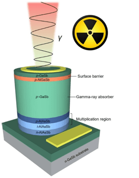 Figure 1. The GaSb/AlAsSb SAM-APD structure.
The research team is led by Prof. Diana L. Huffaker (Department of Electrical and Computer Engineering), Prof. Arion F. Chatziioannou (Department of Molecular and Medical Pharmacology), and Dr. Baolai Liang (California NanoSystems Institute). They bringing extensive experience in semiconductor devices, medical imaging, epitaxial growth to bear on the challenges associated with this project.
Dr. Bor-Chau Juang, the lead researcher, says “The capability of resolving energies in high-energy radiation spectra is mainly determined by the choice of semiconductor materials. We carefully went through all material options at the beginning of this project. We chose GaSb as absorption material because it can offer very good absorption efficiency and efficiently stop high-energy photons due to its high atomic number.”
The devices were grown by molecular-beam epitaxy, an epitaxy method for high-quality of single-crystal semiconductors. “We have over twenty-year experience in compound semiconductor epitaxy. The growth technique for GaSb/AlAsSb heterostructures is built upon our comprehensive understanding of growth mode and material properties,” Dr. Baolai Liang comments, who is the technical director for the MBE user facility at UCLA California NanoSystems Institute.
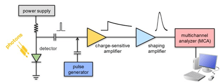
Figure 2. Measurement setup for X-rays and gamma-rays.
“Note that our detectors are actually separate absorption and multiplication avalanche photodiodes (SAM-APDs). This structure is better than PIN photodiode or avalanche photodiode. The avalanching process gives internal gain, which leads to much higher signal-to-noise ratio. In our case, AlAsSb, the large bandgap material, is used to make multiplication regions to generate avalanching, or gain. Additionally, AlAsSb is a perfect option because AlAsSb with a certain composition can be lattice-matched to our absorber material,” says Dr. Dingkun Ren, the co-author and senior researcher.
Dr. Liang adds, “Our work paves the way to achieving efficient detection of high-energy radiations in various applications. We are very excited about our results, and we welcome more collaborations to carry on this research.”
The research was supported by the Defense Threat Reduction Agency (DTRA) and National Science Foundation (NSF) of the United States. The results were published in Advanced Optical Materials (https://doi.org/10.1002/adom.201900107).