Additionally, there is a need for reliable wireless telecommunication technology. Multiple applications require flexible, durable, reliable materials with superior electrical and electromechanical properties.
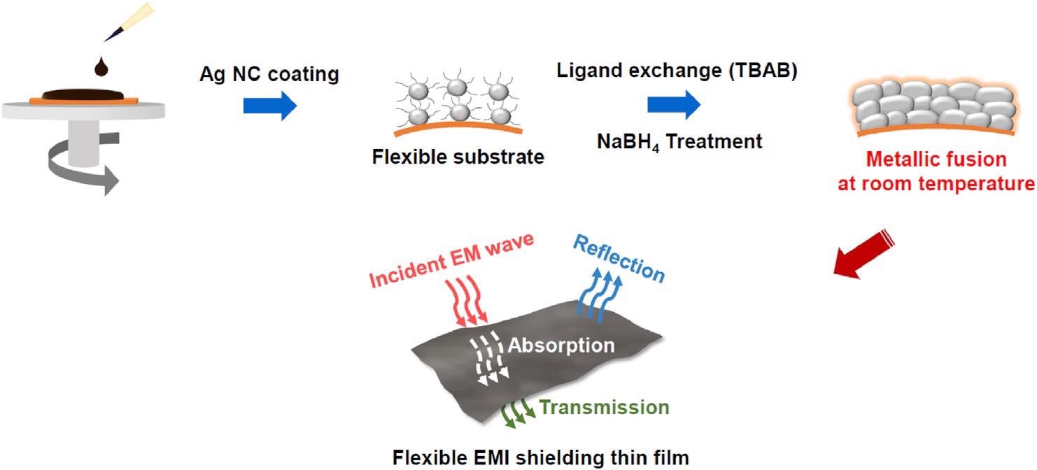
Schematic illustration of the fabrication process of flexible and conductive Ag NC thin film for EMI shielding. Image Credit: Park, S et al., Materialstoday
Interference from electromagnetic radiation is a problem for these technologies that need to be addressed. Therefore, materials which shield against electromagnetic radiation are crucial for the fields of wearable electronics and telecommunication devices.
The rapid deployment of these technologies facilitates the need for low-cost, ultrathin, flexible EMI shielding materials is paramount. These materials need to be able to be applied uniformly over a large area to be effective.
Current EMI Shielding Materials
Currently, many carbon-based, metallic, and conductive polymer materials are used for electromagnetic shielding. However, there are issues with these materials, especially metal-based variants, which include poor adaptability to applications that require significant manual deformation, for example on the moving body of a wearer. Additionally, a lot of energy is required to fabricate materials, which is resource-intensive and has obvious issues with sustainability.
Therefore, the need for materials that can cope with manual deformation and use fewer resources to produce whilst still displaying superior shielding performance has become a central focus of research within the field.
Using Nano-Inks for Shielding Materials
Nano-inks are receiving a lot of attention currently. Fabricated from colloidal silver nanocrystals, these materials display several properties which make them superior candidates for electromagnetic shielding. These materials can be produced at scales that make them suitable for a wide range of commercial applications. Simple chemical processes turn the solutions of silver nanoparticles into large-area, flexible, printable thin films.
However, conventional fabrication methods cause problems with the efficiency of the silver nanocrystal’s charge transfer. Sintering methods can be used to remove insulating organic ligands, but these methods are complex and require high temperatures.
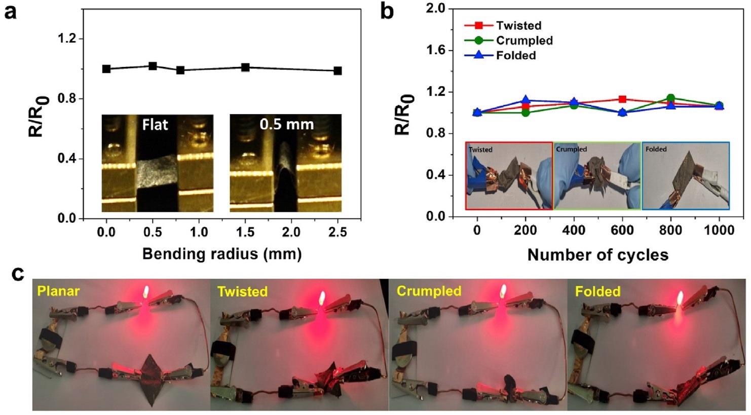
(a) Resistance changes of (AgNC)6 in response to bending radius (0.5, 0.8, 1.5, and 2.5 mm), and (b) repetitive cycles according to various strain forms (crumpled, twisted, and folded) of flexible (AgNC)6. (c) Photographs of flexible (AgNC)6. The red diodes were still lit under various deformations. Image Credit: Park, S et al., Materialstoday
Improving the Process of Silver Nanocrystal Fabrication
Research carried out by a team led by S Park has demonstrated an improved fabrication method for colloidal silver nanocrystals for use as electromagnetic shielding materials. Using a ligand-exchange process to modulate the electromagnetic and electronic properties of the nanocrystals, room temperature and pressure sintering of the nanomaterial is possible.
This leads to the formation of interconnected networks that are large-scale, flexible, and display superior conductivity.
Three-dimensional interconnected structures are formed through metallic fusion and aggregation. Nonmetallic substances that impede efficient charge transfer are eliminated. This significantly improves the properties of the colloidal silver nanocrystals, making them an attractive target for applications that require thin, flexible materials which display superior electromagnetic shielding potential.
The team characterized the material’s optical, morphological, and structural properties using transmission electron microscopy. Additionally, the electromechanical and electrical properties of silver nanocrystal-based materials of different thicknesses were investigated.
Furthermore, mechanical stability and performance were analyzed using endurance tests by deforming the material in different ways. The material showed no significant resistance changes even after 1000 deformation cycles.
To prove the concept, the team used the material to fabricate stable and flexible connections by using a red-light emitting diode.
The results of the study demonstrated that colloidal silver nanocrystal-based materials manufactured via this process displayed superior performance, with a maximum shielding effectiveness of ~60 dB at a thickness of ~ 1.3 µm. Superior conductivity, flexibility, and EMI shielding properties demonstrated that the material is well-suited to wearable and flexible electronic devices.
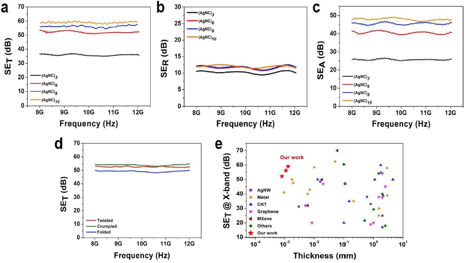
(a) Total EMI SE (SET) (b) reflection SE (SER), and (c) absorption SE (SEA) of Ag NC films versus frequency (from 8.2 to 12.2 GHz) with the different number of repetition. (d) EMI SE changes of (AgNC)6 after diverse deformations. (e) Total EMI SE as a function of thickness for different shielding materials. Image Credit: Park, S et al., Materialstoday
The Future
Wearable and flexible electronics tech is predicted to become commonplace in several key industries such as medicine, mining, the aerospace industry, and the military. Developing materials that can perform well under mechanical stress and keep their integrity with superior electrical properties will be integral to the field and help realize their true potential.
Through developing this novel fabrication process for ultrathin materials based on nanoscale constructs, the team headed by S Park of the Korean Institute of Geoscience and Mineral Resources in the Republic of Korea, the technology has taken a huge step forward.
Further Reading
Park, S et al. (2021) Metallic fusion of nanocrystal thin films for flexible and high-performance electromagnetic interference shielding materials [online] Materialstoday Advances 12 100177. Sciencedirect.com. Available at: https://www.sciencedirect.com/science/article/pii/S2590049821000473
Disclaimer: The views expressed here are those of the author expressed in their private capacity and do not necessarily represent the views of AZoM.com Limited T/A AZoNetwork the owner and operator of this website. This disclaimer forms part of the Terms and conditions of use of this website.