External electric fields are used extensively to control and modify material properties and explore different physical phenomena/effects. The first group of effects is attributed to the carrier density changes induced by the applied electric field at the material surface and identified using field effect transistors (FETs).
The second group of qualitatively different phenomena, such as the bending of the band structure along the applied electric field direction, is attributed to the presence of the electric field within the material. These phenomena are explored using a dual-gate FET with a gate-electrode pair below and above the material under investigation.
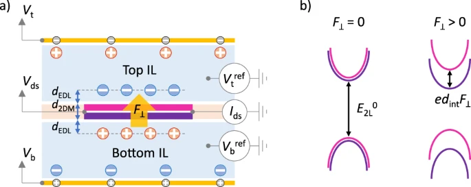
Dual ionic liquid gating. a Concept of a dual ionic liquid-gated bilayer 2DM device. The potentials of the top (Vtref) and bottom (Vbref) ionic liquids (ILs) are independently controlled by the top (Vt) and bottom (Vb) gate voltages. The potential difference between top and bottom ILs drops over a ~2 nm thick layer consisting of two electrical double layers (thickness dEDL) and the bilayer (thickness d2DM), thereby generating an intense electric field (F⊥) through the bilayer. The drain-source voltage (Vds) controls a drain-source current (Ids) through the 2DM. b A band structure sketch of a bilayer 2DM at zero and non-zero electric field. When no field is applied through the bilayer, the band-gap is E2L0. The field breaks the degeneracy between the energy bands corresponding to opposite layers and reduces the overall band-gap by edintF⊥, where dint is the 2DM interlayer distance and e is the elementary charge. Image Credit: Weintrub, B.I et al., Nature Communications
In dual-gate FETs, the potential difference between the top and bottom gate voltages controls the field strength, while the sum of these gate voltages determines the Fermi level.
However, the breakdown of gate dielectrics at a field strength of approximately 0.3 V/nm or one V/nm when measured using local probe techniques in conventional solid-state FETs limits their effectiveness in studying large electric fields.
Ionic gating, which combines electrochemistry with condensed matter physics, can be used to overcome this limitation. In this method, an ionic compound, typically ionic liquid (IL), is placed over the material under investigation.
The potential applied between the sample and the gate electrode in the liquid drops over a less than one nm thick electric double layer (EDL), modeled as a capacitor with an extremely large geometric areal capacitance of 10 μF/cm2, at the sample/IL interface.
A carrier density is induced inside the material by the resulting electric field within the EDL. The field generated using the ionic gating approach remains unaffected by the dielectric breakdown of gate electrics.
However, the electrochemical modification of the electrodes or material that occurs during a substantial potential drop across a specific sample/IL interface is the only major limitation of this approach.
Carrier densities larger than 1014 cm−2, which were previously unrealizable, can be realized using the ionic gating approach. Electronic phases, such as gate-controlled ferromagnetic, exotic superconductivity, and structural phase transitions, can occur due to interactions between electrons at such carrier densities.
These phenomena are more noticeable in 2DMs, including phosphorene, transition metal dichalcogenides (TMDCs), or graphene, as the carriers in these materials are spatially confined to a few or single atomic layers.
Although ionic gating can induce high carrier densities in materials, dual ionic gating has not been utilized to generate strong external electric fields in the bulk of materials, specifically 2DMs.
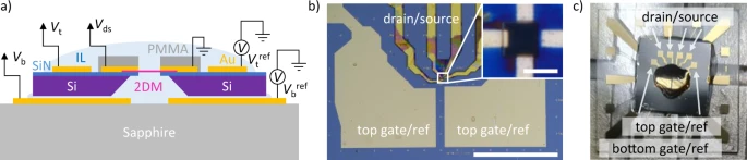
Device and measurement overview. a Side-view cartoon of the device and measurement scheme. The 2D material (2DM) is suspended over a hole in a silicon nitride (SiN) membrane grown on a silicon (Si) substrate. Gold (Au) electrodes are used to electrically contact the device, and cross-linked PMMA resist covers the drain/source electrodes. All voltages are defined as in Fig. 1. b Microscope (5x) image of sample #1 before applying ionic liquids. Drain and source electrodes are covered with cross-linked PMMA. Scale bar is 1 mm. Inset: 100x image of the 2DM deposited onto a square hole (~4 μm × 4 μm) in SiN. Everything in the inset other than the area of the 2DM over the hole is covered by cross-linked PMMA. Scale bar is 4 μm. c Photograph of sample #1 before measurement. Note that the top and bottom ionic liquids are not in contact. Image Credit: Weintrub, B.I et al., Nature Communications
The Study
In this study, researchers used the dual ionic gating approach to generate intense electric fields in single-layer (1L), bilayer (2L), and few-layer tungsten diselenide (WSe2) FETs. Later, they determined the band gap and quantified the field strength in these 2DMs using a combination of electrical transport and electrochemical measurements.
Device Concept
The objective of the experiment was to generate large perpendicular electric fields in an electrically-contacted 1L/2L/few-layer 2DM suspended between two IL volumes and measure them. The potential difference between the top IL and bottom IL/ΔVref was controlled independently using the top and bottom gate voltages, respectively.
This potential difference dropped over an ultrathin layer composed of two EDLs and a 1L/2L/few-layer 2DM generated an intense electric field through the 2L/few-layer material. Additionally, the drain-source current through the 2DM was controlled by the drain-source voltage.
A potential difference was applied between the two ILs/diethyl methyl(2-methoxyethyl)ammonium bis(trifluoromethylsulfonyl)imide (DEME-TFSI) below and above the 2DMs to generate the electric field within the 2DM.
Researchers calculated the charge inside charge-neutral 2DM by approximating the ΔVref as five V considering the electrochemical window limits of the IL used in the study and the dielectric constant of 2DM/WSe2 and EDL as 7.5 and 15, respectively.
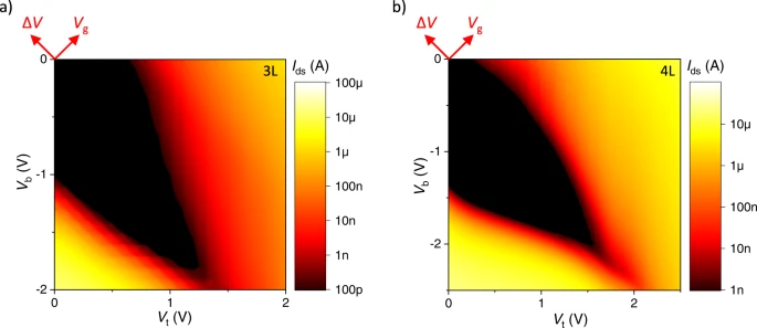
Transport in trilayer and quadlayer WSe2. Map of Ids vs. (Vb, Vt) for a 3L WSe2 (sample #2) and b 4L WSe2 (sample #3). As |ΔV| increases from 0 V, the band-gap region (black) shrinks, and it eventually closes at a critical value of F⊥ around 1.4 V/nm and 0.9 V/nm for the 3L and 4L device, respectively. Image Credit: Weintrub, B.I et al., Nature Communications
Observations
Dual IL-gated FET was fabricated successfully using conventional 2DM processing techniques. The overall band-gap was reduced by edintF⊥, where e represented the elementary charge, while dint and F⊥ represented the 2DM interlayer spacing and electric field, respectively.
In the 2L WSe2 device, the band-gap decreased linearly with the increasing difference between the bottom and top IL gate voltages/ΔV and reduced to zero at ΔV ≈ 5.9 V, which was larger than the electrochemical window of the used ILs.
However, a larger band-gap reduction was observed at a much lower ΔV value in few-layer WSe2 compared to bilayer WSe2 due to a larger drop in ΔVref with the increasing number of layers in WSe2.
The stronger response of few-layer WSe2 to ΔVref resulted in an electric field-driven semiconductor-to-metal transition. For instance, the band-gap closed at ΔV ≈ 4 V in both trilayer (3L) and quad layer (4L) WSe2, which was within the IL electrochemical window.
The few-layer WSe2 band structure was approximated as energy-degenerate valence and conduction bands, with one set of bands for each layer. An application of an external perpendicular electric field broke the 2DM inversion symmetry and induced a maximum energy difference between the 2DM outer layers. Thus, the few-layer WSe2 band-gap became spatially indirect that occurred between one layer’s valence band and another layer’s conduction band.
In the 2L and 1L devices, the field strength achieved at ΔVref ≈ 5V was 2.5 ± 0.3 V/nm and 4.0 ± 0.4 V/nm, respectively. However, the band-gap in three-layer and quad-layer devices demonstrated a stronger dependence on the generated electric field, with the band-gap closing at 1.4 V/nm and 0.9 V/nm, respectively.
The electric field generated in the 1L device surpassed the dielectric strength of the common gate dielectrics such as hafnium (IV) oxide, silicon nitride, and hexagonal boron nitride.
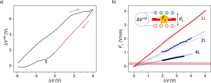
Electric field through 1L, 2L, and 4L WSe2. a Reference voltage data from 1L WSe2 (sample #4). The direction of the sweep is indicated by arrows, and the red portion of the curve is used to extract the field. b Perpendicular electric field through 1L WSe2 extracted from reference voltage data (red data points) alongside the 2L and 4L WSe2 field data extracted from transport maps (blue and dark blue dots, respectively) and fits to these data points (solid lines). Dashed lines for 2L and 4L devices represent the field values from estimated reference voltage, ΔVref = αΔV, for the respective devices. The red-shaded region from 0.1 to 0.3 V/nm shows the maximum field strength in conventional dielectric devices. The cartoon inset illustrates the relation between the potential difference of top/bottom ILs and the field across the device, F⊥ = ΔVref/d⊥. Image Credit: Weintrub, B.I et al., Nature Communications
The 4 V/nm field strength in the 1L device was sufficient to induce several predicted yet unobserved structural and electronic phases in different 2DMs. The maximum field strength in 2L WSe2 and 3L/4L WSe2 were limited by the IL electrochemical window and the material utilized to quantify the field strength, respectively.
Larger fields can be realized using ILs with smaller double-layer thickness and/or thinner 2DMs, by increasing the ΔVref using ILs with larger electrochemical windows or by measuring the field using large band-gap materials.
To summarize, the findings of this study demonstrated the feasibility of using an EDL composed of IL/2DM/IL in place of a conventional IL/metal electrochemical system to investigate the dielectric breakdown of materials and explore diverse physical phenomena in intense electric fields. Moreover, this dual IL-gated design will be compatible with different 2DMs/other thin materials, several ionic compounds such as polymer electrolytes and ionic gels, and ILs.
Disclaimer: The views expressed here are those of the author expressed in their private capacity and do not necessarily represent the views of AZoM.com Limited T/A AZoNetwork the owner and operator of this website. This disclaimer forms part of the Terms and conditions of use of this website.