Image Credit: Institute of Industrial Science, The University of Tokyo.
3D integrated circuits are made up of numerous layers, each of which contributes to the overall function. Because they can be produced at relatively low temperatures while possessing high carrier mobility, minimal charge leakage, and the ability to tolerate high voltages, oxide semiconductors are gaining popularity as materials for numerous circuit components.
There are also advantages to employing oxides rather than metals in operations where electrodes may be exposed to oxygen and become oxidized during the integration process.
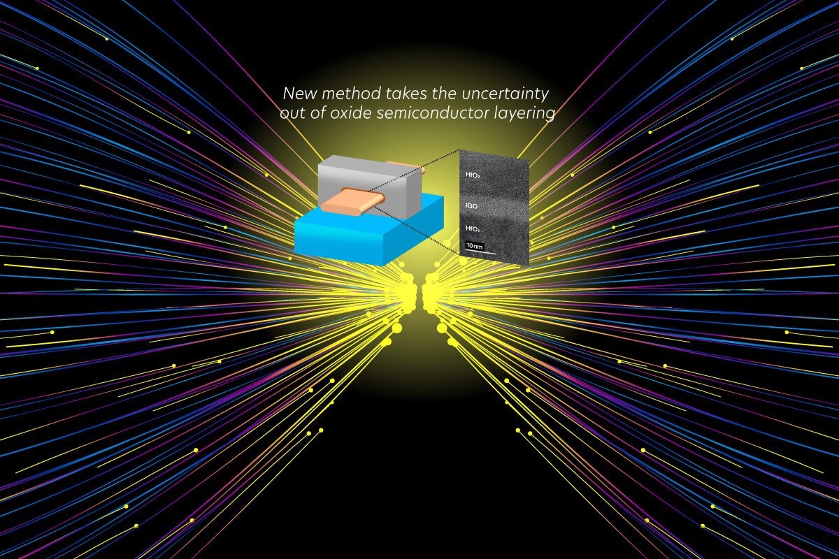
However, developing the processes required to successfully deposit very thin layers of oxide semiconductor materials in the manufacturing of devices is difficult and has yet to be thoroughly established. The researchers recently published a paper on an atomic layer deposition (ALD) technology that yields layers suitable for large-scale integration.
Using our process, we carried out a systematic study of field effect transistors (FETs) to establish their limitations and optimize their properties.
Kaito Hikake, Study Lead Author, Institute of Industrial Science, The University of Tokyo
FETs regulate the flow of current in a semiconductor. “We tuned the ratio of the components and adjusted the preparation conditions and our findings led to the development of a multi-gate nanosheet FET for normally-off operation and high reliability,” Kaito Hikake notes.
The results showed that a FET manufactured from the selected oxide semiconductor via ALD performed the best. The multi-gate nanosheet FET is thought to be the first to integrate high carrier mobility, reliability, and normally-off operation.
In rapidly moving areas such as electronics, it is important to translate proof of concept findings into industrially relevant processes. We believe that our study provides a robust technique that can be used to produce devices that meet the market's need for manufacturable 3D integrated circuits with high function.
Masaharu Kobayashi, Study Senior Author, Institute of Industrial Science, The University of Tokyo
The results of this study have offered a solution to one of the major challenges in the manufacture of semiconductor-based electronic devices. Hopefully, this will lead to more designs of high-functioning electronics becoming actual products.