From single flakes to printed films, researchers tracked how thickness and air exposure reshape the electrical behavior of one of the thinnest titanium-based MXenes.
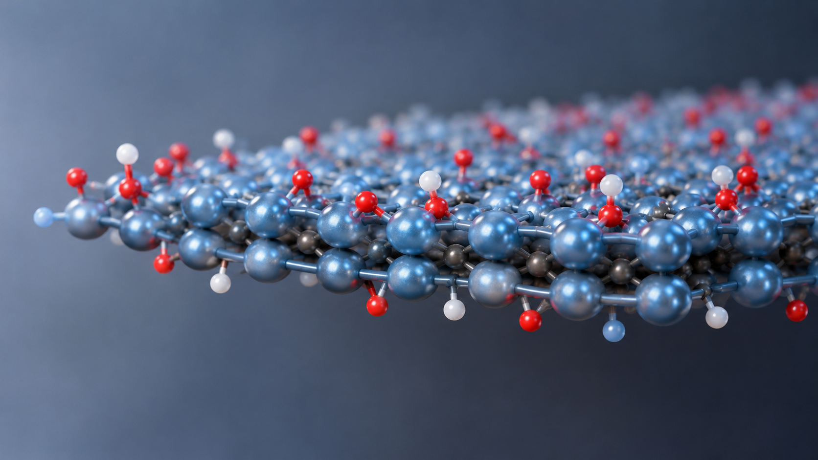
Paper: Tunable charge transport in Ti2CTx MXene flakes and printed thin films: a route to designing high-performance MXene devices. AI-generated abstract conceptual image created using ChatGPT/OpenAI
*Important notice: This news reports on an unedited version of an accepted paper and is awaiting final editing. Therefore, the paper should not be regarded as conclusive or treated as established information.
In a recent research article published in the journal npj 2D Materials and Applications, researchers systematically investigated how thickness-dependent oxidation affects charge transport in Ti2CTx MXene flakes and printed thin films, establishing design principles for high-performance, air-sensitive MXene electronic devices.
MXene Oxidation and Transport
Flexible and wearable electronics increasingly use two-dimensional (2D) materials, particularly those that can be processed into inks suitable for printing techniques.
Among these, MXenes, 2D transition metal carbides, nitrides, and carbonitrides, have attracted attention because of their metallic conductivity, unique surface chemistry, and hydrophilicity.
MXenes have the general formula Mn+1XnTx, where M is an early transition metal (such as Ti), X is carbon and/or nitrogen, and Tx represents surface terminations like –O, –OH, and –F. Ti-based MXenes, especially Ti3C2Tx, have been well explored as inks for printed electronics because of their high conductivity and ease of fabrication into thin films.
However, oxidation of MXene surfaces upon exposure to air and moisture remains a challenge, causing substantial changes in charge-transport behavior, particularly in ultrathin flakes.
The thinnest member of the Ti-based MXene family, Ti2CTx, has a minimal layered structure and high surface-to-volume ratio, but is more vulnerable to oxidation than thicker analogs. Understanding how oxidation and layer thickness affect electrical properties is important for tailoring MXene inks suitable for high-performance printed electronics.
Ti2CTx Synthesis and Characterization
The study used selective etching of the Ti2AlC MAX phase with a mild protocol combining HCl and LiF (the in-situ HF method), followed by a minimally intensive layer delamination (MILD) technique. This approach is gentler than aggressive HF etching and sonication-based delamination and produces micron-sized flakes with fewer defects.
The resulting MXene suspensions were analyzed using several techniques to assess successful etching, structure, and composition. Optical absorption spectroscopy identified characteristic peaks associated with Ti2CTx electronic transitions, while X-ray diffraction (XRD) verified the successful removal of aluminum from the precursor MAX phase.
Scanning transmission electron microscopy with energy-dispersive X-ray spectroscopy (STEM-EDX) mapped elemental distributions, confirming that residual aluminum was negligible. Raman spectroscopy distinguished vibrational modes between the MAX phase and etched MXene films, indicating etching-induced structural changes.
X-ray photoelectron spectroscopy (XPS) revealed the chemical states of titanium and carbon, including surface oxidation species and functional groups. Atomic force microscopy (AFM) assessed flake thickness and lateral size distribution on substrates, providing a statistical overview of the flake population relevant to transport measurements.
Devices were fabricated by spin-coating highly diluted Ti2CTx suspensions on SiO2/Si substrates to isolate single flakes, while thin films were produced separately by spray coating. Individual flake devices were encapsulated with PMMA shortly after deposition to limit further oxidation exposure.
Electrical transport measurements at room temperature were performed on flakes with different thicknesses (single layer, bilayer, few-layer, and multilayer) and on spray-coated thin films.
Detailed temperature-, magnetic-field-, and gate-voltage-dependent transport measurements then focused on two multilayer flakes and a spray-coated film because single-layer and highly resistive bilayer devices were not suitable for reliable low-temperature measurements.
Thickness-Dependent Charge Transport
Optical and structural characterization indicated well-crystallized Ti2CTx flakes with low residual aluminum and limited processing-induced defects, supporting comparisons between material properties and transport behavior.
AFM statistics indicated single-layer Ti2CTx flakes had a thickness of around 1.8 nm, including interlayer spacing, in ambient measurements, while STEM-EELS gave about 1.4 nm.
The apparent AFM thickness distribution peaked near 3.45 nm, but after accounting for adsorbate effects, the authors concluded that about 72% of the suspension consisted of single-layer and bilayer flakes.
XPS identified Ti–O species associated with oxidation, while STEM-EDX and STEM-EELS provided the main evidence that thinner regions contained more oxygen relative to Ti and were more oxidized.
Electrical conductivity strongly depended on thickness: monolayer flakes underwent extensive oxidation and became insulating, with resistance above the measurement limit; their low-temperature hopping regime was not directly measured. Bilayer and thicker flakes retained finite conductivity because oxidized outer layers partially shielded locally metallic inner regions.
Temperature-dependent transport measurements revealed different regimes according to oxidation level. The spray-coated film followed 2D Mott variable-range hopping (VRH) across the measured temperature range.
Multilayer flakes showed low-temperature VRH followed by nearest-neighbor hopping (NNH) or stronger thermal activation at higher temperatures. In the least-oxidized multilayer, an intermediate power-law critical regime indicated proximity to the metal-insulator transition rather than fully metallic transport.
For spray-coated films, the network contained both intra-flake and inter-flake hopping pathways. At low temperature, intra-flake VRH within metallic grains remained the dominant, rate-limiting process; near room temperature, inter-flake hopping became increasingly limiting as oxidized junctions added resistance.
Design Insights for MXene Devices
This work uses Ti2CTx MXene as an effective model system to understand and control how oxidation, thickness, and charge transport relate in 2D material inks for printed electronics.
The study treats oxidation as a controllable design parameter that researchers can adjust through flake selection and processing, helping tune conductivity or semiconducting behavior for different applications.
The methodologies, material insights, and transport models presented provide design guidance for air-sensitive 2D material inks.
The authors propose using thickness sorting and deposition control to favor minimally oxidized few-layer and multilayer flakes for high-conductivity uses such as antennas, electromagnetic shielding, electrodes, and contacts, or thinner and more oxidized flakes for switching, photodetectors, and gas sensors.
These are proposed application routes, not devices demonstrated in the study.
Source:
- Wu S., Piatti E., et al. (2026). Tunable charge transport in Ti2CTx MXene flakes and printed thin films: a route to designing high-performance MXene devices. npj 2D Materials Applications. DOI: 10.1038/s41699-026-00748-4, https://www.nature.com/articles/s41699-026-00748-4