Structured substrates are increasingly used in semiconductor research. Gaining insights into the inherent strain and crystalline properties of device structures becomes critical to meet the device quality and reliability. X-ray diffraction is generally used to analyze strain states, lattice constants, film thicknesses of layer structures and scanning electron microscopy (SEM) is employed to analyze surfaces and defects in the structure to gain knowledge about the growth history.
This article presents the results of 3D confocal Raman imaging measurements, which provide information about strain and changes in the lattice structure by revealing changes in the signal.
Sample Description and Experimental Procedure
The sample analyzed was a 20µm-thick unintentionally doped GaN layer grown by metal organic vapor phase epitaxy (MOVPE) and ubsequent overgrowth by hydride vapor phase epitaxy (HVPE) on a c-plane patterned sapphire substrate (PSS). I-line beam stepper lithography was employed to pattern the sapphire substrate utilizing a KMPR 1000 negative photoresist and ion-coupled plasma (ICP) etching. The honeycomb-like structure under analysis has 12µm of pitch, 3.5µm of ridge width, and 4.5µm of trench depth.
An alpha300R+ confocal Raman microscope equipped with a frequency-double Nd:YAG laser for excitation (λ=532nm) was used for the sample analysis. A single-mode fiber was used to couple the light into the microscope, and a dichroic mirror and a 100x NA 0.9 air objective were used to bring the light onto the sample. An edge filter was used to filter out the Rayleigh-scattered light in the detection beam path. To achieve good depth resolution without compromising the collection efficiency, a 50µm core-diameter fiber was employed as a confocal pinhole.
The light was then brought onto a UHTS300 spectrometer featuring an1800g/mm grating (BLZ 500nm) and an EMCCD camera. A piezoelectric scanning stage was used to achieve the XY positioning of the sample, with excellent focus control (10nm single step) by a stepper motor. The Raman spectra were collected as a depth scan along an interesting axis of the sample (240x80 points on a scan area of 60x20µm2), as depicted in Figures 1 and 2.
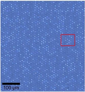
Figure 1. Stitched image of the sample acquired using a 100x objective. The red square shows the position of the high resolution video image shown in Figure 2.
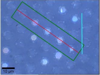
Figure 2. Video image of the area of interest. The area of the stack scans is shown in green and the red line shows the position of the single depth-scan.
3D stack scans were additionally carried out and studied (180x45x20 points with a scan volume of 60x15x20 µm3). For each of the scans, a spectrum was collected at every pixel using an acquisition time of 20 ms/spectrum. The information relevant to the spectra was extracted and presented as color-coded Raman images using the WITec Project Plus data analysis software. The results allowed for the creation of a 3D image of the Raman features across the sample volume of interest.
Experimental Results
Analysis of Different Spectral Features in the Sample
Three areas could be detected in the sample using a depth-scan. Figure 3 illustrates the false-color Raman image with the spectra pertaining to colors depicted in Figure 4. The spectrum reveals the characteristic features of GaN spectra in the magenta areas. An enhanced fluorescence can be observed in the green areas, which coincide with the edges of the ridges.
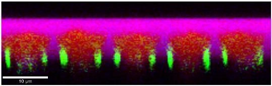
Figure 3. Color-coded Raman image of the depth scan performed along the red line shown in Figure 2. The magenta, red and green areas correspond to the spectra shown in Figure 4.
As can be seen in the green spectrum in Figure 4, the fluorescence is positioned predominantly in the low-wave number range of the spectrum. The holes in the structure were positioned exactly underneath the red areas. The height of the structure seems to be decreased because of the difference in the refractive index between air (~1) and GaN (2.45).
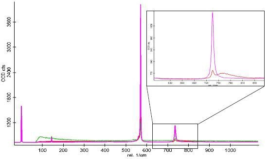
Figure 4. Color-coded Raman spectra corresponding to the Raman image shown in figure 5. In the zoomed view the green spectrum is omitted for clarity.
The red areas can be spectrally characterized by a significant reduction of the intensity of the peak close to 735 rel.1/cm, but with a broad peak on the higher wavenumber side of this peak (Figure 4). This peak shift and broadening may suggest that the material is of lower crystalline quality. The inclusion of contaminants in non-c-planar growth at these positions could provide the coupled non-planar optical phonons A1(LO)+ or A1(L) +.
Figure 5 depicts one layer extracted from the stack scan wherein the characteristic spectral features are presented in the same color code as in the earlier images. It is readily apparent that the location of the fluorescence (green areas) is at the walls of the ridges and that the areas of lower intensity of the 735 rel.i/cm peak (red areas) are on the inside of the holes. The honeycomb-like holes in the structure were located accurately underneath the red areas and the yellow color is a combination of the red and the green areas.
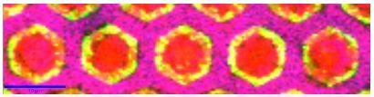
Figure 5. Color coded Raman image of a single plane extracted from the stack scan. The magenta, red and green domains correspond to the spectra shown in Figure 4.
The layers captured in the image stack were analyzed in the same manner of the layer depicted in Figure 5 and integrated into a 3D reconstruction using the Image J software. Figure 6 delineates a 3D view of the reconstructed 3D structure. As show in Figure 5, the position of the fluorescence and the regions of a weaker 735 rel.1/cm peak can be clearly determined at positions of the holes.
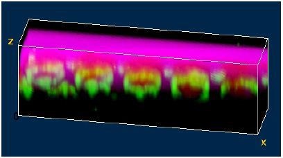
Figure 6. Color-coded 3D Raman Image of the structure. The colors correspond again to the colors of the spectra shown in Figure 4.
Peak-Shift Analysis
A peak-shift analysis of the spectra was conducted using the aforementioned results. For this analysis, a Lorentzian curve was used to fit the peak close to 570rel.1/cm of each spectrum in each of the scans. This helps determining the position of the Raman peaks accurately with a typical uncertainty of 0.02rel.1/cm. Figure 7 illustrates the position of this peak for the depth-scan and Figure 8 shows two representative spectra demonstrating the peak shifts.
Figure 7. Color-coded Peak-Shift Image of the structure as measured using a depth scan. The shift of the main peak is shown in this image.
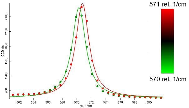
Figure 8. Spectra illustrating the peak shifts. The data points as well as the fitted curve are displayed in the colors corresponding to Figure 7.
Figure 9 delineates the distribution within the sample in one of the planes extracted from the stack scan, showing various domains. Nevertheless, these discrete images in single planes are inadequate to gain information about the peak shift and the resulting strain distribution in the sample. A much clearer analysis is possible by performing a 3D reconstruction utilizing the entire data acquired by the stack scan.
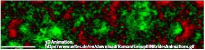
Figure 9. Color-coded Peak-shift Image of the structure extracted from one layer of the stack scan. The shift of the main peak is shown in this image.
Figure 10 demonstrates this 3D distribution with shifts to lower wave numbers again shown in green and shifts to higher wave numbers represented in red. The image beneath is the intensity of the peak near 735rel.1/cm of a plane just above the holes and considers the spatial association of the stress fields with the position of the holes. It can be clearly seen that the stress fields propagate from the interface to the surface predominantly in tube-like structures, which was not clear in the 2D images of the sample.
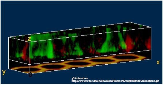
Figure 10. 3D View of the stress fields. The image in the bottom plane shows the intensity of the peak near 735rel.1/cm in an orientation showing where the holes in the structure are located.
Conclusion
The results clearly demonstrate the advantage of using 3D confocal Raman imaging to study Group III nitrides.

This information has been sourced, reviewed and adapted from materials provided by WITec GmbH.
For more information on this source, please visit WITec GmbH.