Electron Backscatter Diffraction (EBSD), a scanning electron microscope (SEM)-based method, is widely used for microstructural characterization of materials. EBSD is a surface method that involves electron diffraction taking place within a few tens of nanometers of the sample surface.
Any residual surface deformation or reaction product layers from standard sample preparation methods negatively affect EBSD pattern generation. Therefore, careful sample preparation is crucial for successful EBSD materials characterization.
This articles discusses the application of Broad Beam Ion Milling to generate improved quality of data from magnesium, zirconium, aluminum, titanium alloys and galvanized zinc coatings, which pose challenge to sample preparation by mechanical methods.
Experimental Procedure
All samples excluding the galvanized zinc were placed in bakelite and subjected to mechanical polishing to obtain colloidal silica finish. Then, Fischione Instruments' Model 1060 SEM Mill was used to ion mill the samples using a large ion beam (5mm) for removing the residual surface deformation. Milling of the galvanized surface was performed until the substrate became visible.
A FEG SEM was used to analyze the milled specimens, which were then characterized by EBSD/EDS methods using Oxford Instruments' Symmetry EBSD detectors equipped with the AZtec software.
Experimental Results
This article presents the results obtained for the materials, including zirconium, titanium, magnesium, galvanized steel, and aluminum. For EBSD characterization, zirconium and its alloys need to be prepared by careful chemical/attack polishing utilizing aggressive acids.
Figure 1 depicts an SEM backscattered image from the ion milled sample after standard metallographic attack polishing.

Figure 1. SEM BSE image after ion milling. Image Credit: Oxford Instruments
Figure 2 shows an EBSD pattern and Figure 3 illustrates an EBSD inverse pole figure colored map, while Figure 4 depicts a corresponding pole figure. Table 1 summarizes EBSD acquisition data along with a comparison of grain size and Kearn's factors employed to measure textures in zirconium alloys at different binnings used for mapping the same area.

Figure 2. EBSD pattern from zirconium. Image Credit: Oxford Instruments

Figure 3. EBSD IPF. Image Credit: Oxford Instruments
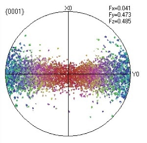
Figure 4. EBSD (0001) pole figure. Image Credit: Oxford Instruments
Table 1. Details of EBSD and the respective microstructural parameters. Source: Oxford Instruments
| |
4x4 |
6x6 |
8x8 |
| speed Hz |
550 |
733 |
850 |
| acq time (mins) |
95 |
69 |
61 |
| hit rate % |
95.7 |
87.5 |
92.7 |
| mean grain size (μm) |
5.00 |
5.19 |
5.00 |
| min grain size (μm) |
0.202 |
0.202 |
0.202 |
| max grain size (μm) |
19.47 |
17.39 |
19.36 |
| total grains |
3740 |
3594 |
3731 |
The results clearly show the achievement of high speed mapping and hit rates following ion milling.
For EBSD characterization, careful mechanical polishing is required for titanium and its alloys. Figure 5 shows a forescatter image from an ion milled titanium sample with a typical EBSD pattern, as shown in Figure 6. Figure 7 depicts an EBSD inverse pole figure colored map, while Figure 8 shows a corresponding pole figure. Table 2 shows EBSD acquisition details.
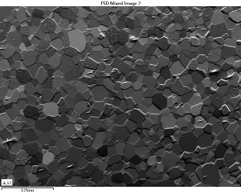
Figure 5. Forescatter detector image. Image Credit: Oxford Instruments

Figure 6. ESBP. Image Credit: Oxford Instruments
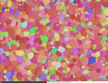
Figure 7. 8x8, 864Hz, 19nA. Hit rate 97.6 %. Time 79min. Image Credit: Oxford Instruments
Table 2. Details of EBSD and the respective microstructural parameters. Source: Oxford Instruments
| |
8x8 |
| speed Hz |
864 |
| acq time (mins) |
79 |
| hit rate % |
97.6 |
| mean grain size (μm) |
33.05 |
| min grain size (μm) |
2.034 |
| max grain size (μm) |
96.96 |
| total grains |
809 |
| (0001)fz |
Fz=0.632 |
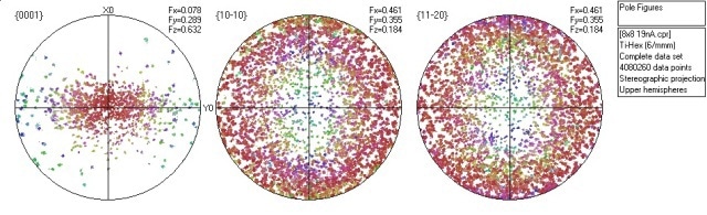
Figure 8. EBSD (0001) Pole figure. Image Credit: Oxford Instruments
For magnesium and its alloys, mechanically polished surfaces can be used successfully for ion milling for EBSD characterization. An SEM backscattered image obtained from the ion milled is shown in Figure 9, with a typical EBSP as illustrated in Figure 10.
Figure 11 depicts an EBSD inverse pole figure colored map, while Figure 12 shows a corresponding pole figure. Table 3 summarizes the conditions applied for EBSD acquisition. The results clearly show the achievement of high speed mapping and hit rates after ion milling.

Figure 9. SEM BSE image after ion milling. Image Credit: Oxford Instruments

Figure 10. EBSD pattern from magnesium. Image Credit: Oxford Instruments
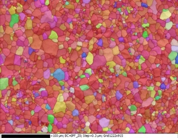
Figure 11. EBSD IPF map after ion milling. Image Credit: Oxford Instruments
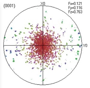
Figure 12. EBSD (0001) pole figure. Image Credit: Oxford Instruments
For galvanized steel, ion milling was performed on the galvanized surface devoid of any surface preparation. Some indexing problems were caused by topography from the original surface, but sample preparation was successful for EBSD characterization, as depicted in the EBSD from the steel and zinc coating illustrated in Figure 13.
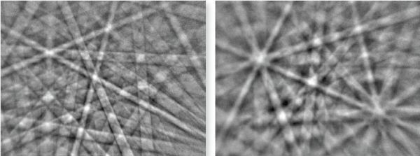
Figure 13. EBSD pattern from a) steel and b) zinc. Image Credit: Oxford Instruments
EBSD mapping was performed on a region that comprised both the substrate and the galvanized coating. Such a region is delineated in a series of EBSD pattern quality, phase and IPF colored maps in Figure 14. These maps clearly demonstrate the advantage of sample preparation by ion milling for EBSD characterization.
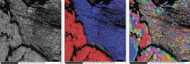
Figure 14. EBSD a) pattern quality, b) phase (red=steel/ferrite, blue=zinc) and c) IPF maps from a region with both the steel substrate and the zinc coating. Image Credit: Oxford Instruments
Careful mechanical preparation is crucial for aluminum and its alloys for successful EBSD characterization. The example shown here is an ion milled aluminum alloy after mechanical polishing. Figure 15 depicts a typical EBSD pattern and Figure 16 illustrates an IPF colored map, while Figure 17 shows a corresponding pole figure.

Figure 15. EBSP. Image Credit: Oxford Instruments
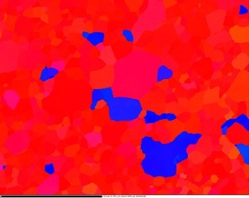
Figure 16. IPF colored map. Image Credit: Oxford Instruments
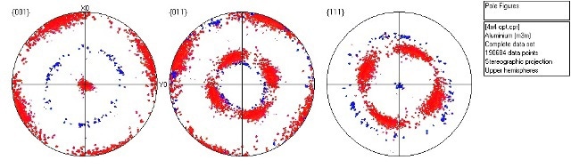
Figure 17. Pole figures. Image Credit: Oxford Instruments
Conclusion
The results clearly demonstrate the advantage of using ion milling for preparing materials such as zinc, magnesium, and zirconium for EBSD characterization. Moreover, the very high quality sample surfaces achieved through this approach enables rapid acquisition of EBSD data from low symmetry structures.

This information has been sourced, reviewed and adapted from materials provided by Oxford Instruments.
For more information on this source, please visit Oxford Instruments.