| Finding the grain boundaries in materials is vital because the material’s grain structure very often defines its mechanical properties. An example is given in the Hall-Petch relation, where strength is inversely dependent on the square root of the grain size. Grain size is also important for quality control and for optimising structures, but for some materials, it can be difficult to reveal the grains. Factors Complicating Conventional Grain Size Analysis Complications arise when the grain boundaries are indistinct or incomplete as in figure 1 where all the grain boundaries have not etched equally well. There are vague hints of the missing boundaries near the centre of the image and sharp corners on adjacent, visible boundaries. It is possible that the etchant has not attacked these boundaries because they are low angle boundaries or they do not have small particles decorating them. In this case, conventional mean linear intercept measurements would overestimate the grain size because some grains would be combined together and appear to be larger than they really are. | 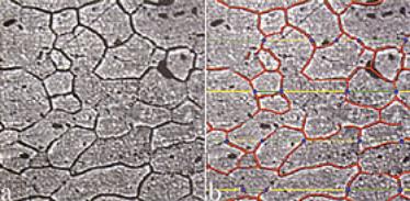
| | Figure 1. (a) An etchant has not revealed all the grain boundaries in this sample of 6061 aluminium alloy. (b) The visible grain boundaries have been marked in red, and linear intercept measurements as blue dots. | New Techniques for Measuring Grains New techniques based on the electron microscope, such as orientation/channelling contrast imaging and electron backscatter diffraction (EBSD), offer useful alternatives to conventional metallographic methods. The ability of these new methods to relate crystallography and microstructure is extremely useful for measuring multiphase, deformed and difficult materials. However they can be slower than existing methods and can generate too much information. Digital Imaging Tips For accurate measurement of grain size from digital images, a good rule of thumb is that the grains should be at least 20 pixels wide. It is also essential to know the smallest grain that can be measured, and to record this lower size threshold as it can bias the grain size statistics. Choosing an appropriate magnification is also critical. Accuracy of Grain Size Determination Techniques A study was conducted recently at NPL comparing different systems and techniques for grain sizing, by measuring a deformed and partially recrystallised Nimonic 901 specimen. Uncertainties (95% confidence) were found to be 40% in recrystallised grain size, about 100% in unrecrystallised grain size, and approximately 20% in volume fraction recrystallised. NPL is currently working in collaboration with AEA Technology and Sheffield Hallam University, with input from materials suppliers and users, to improve measurement practice for grain size and size distribution. Channelling Contrast Imaging Channelling contrast is produced in the scanning electron microscope (SEM) when a suitable specimen and backscatter detector geometry allow channelling of the electron beam by the specimen. Different grain orientations channel to different extents, resulting in the grains appearing as different shades of grey. Channelling contrast images take only minutes to acquire and can be very sensitive to small changes in orientation, so they can image sub-grains and deformed or unrecrystallised regions in materials. However, they can be blind to changes in orientation that happen to produce similar signal levels, and cannot always distinguish between grains and sub-grains. Electron Backscatter Diffraction Electron backscatter diffraction, a technique based on the SEM, uses a stationary electron beam that interacts with a tilted specimen (fig 2) to produce an electron backscatter diffraction pattern (EBSP). EBSPs have a beauty and symmetry that is unique and fascinating, but more importantly they provide full crystallographic and phase information that can be directly related to microstructure at sub-micrometre resolution. | 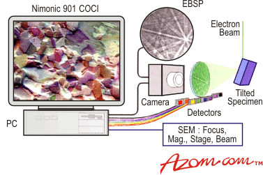
| | Figure 2. The production of an electron backscatter diffraction pattern and a colour orientation contrast image from a deformed and partially recrystallised Nimonic 901 specimen. The COCI image is approximately 150µm wide. | An EBSP system can also be used to scan a region of a specimen to produce an orientation map (OM). Scanning is usually done by either moving the specimen or the electron beam; at each point an EBSP is generated and analysed, and the phase, orientation and location data stored. Figure 3 shows a channelling contrast image (top left) and an EBSP orientation map (bottom right) produced from a deformed and partially recrystallised Nimonic 901 specimen. The unrecrystallised regions have a mottled appearance. | 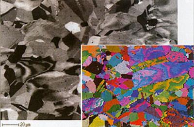
| | Figure 3. Channelling contrast image and orientation map from a deformed an partially recrystallised Nimonic 901 specimen. Unrecrystallised regions have a mottled appearance. | Limitations of Electron Backscatter Diffraction One problem with EBSP, however, is that the specimen has to be sharply tilted, usually 60-70° from the horizontal. This can cause focusing problems and stretch or distort the image. For reliable measurement of grain size, calibration of the SEM magnification (using a standard traceable to National standards), both vertically and horizontally, is critical. Changing the working distance (by refocusing) can invalidate the magnification and EBSP calibrations and introduce errors into the orientation measurements. The main drawback with the automated EBSP mapping technique is speed. Most systems can produce an orientation measurement in about a second, so a 200 - 200 (40,000 point) image will take about 11 hours. EBSPs that cannot be indexed may increase this time. A system that is probably the fastest in the world takes just under 0.2 s per image, and applies an image correlation algorithm to successive EBSPs for speed, but even at this rate, accurate measurement of grain size may not be practical because of the low resolution of the images that can be produced. In real materials it is not possible to analyse (or index) every EBSP and this unavoidable problem produces missing data in the map, e.g. from other phases, grain boundaries, scratches and dirt. Small regions of black (figures 3) represent missing data. By using extrapolation techniques, small regions of missing data can be estimated and filled in. Orientation Contract Imaging Orientation contrast imaging (OCI) is similar to channelling contrast imaging, except an EBSP geometry is used with several detectors positioned below and around the EBSP phosphor (fig 2). This makes the overall signal smaller, but it produces an image that changes with the position of the backscatter detector, which is not usually the case with conventional channelling contrast. Colour Orientation Contract Imaging A colour OCI (COCI) is a combination of images from three detectors using intensities of red for the first image, green for the second, and blue for the third. Examples of COCIs are given in figure 2. With a COCI, the grains are highly visible, as it is unlikely that adjacent grains will have the same colour. Because a COCI uses the EBSP geometry it is possible to measure the orientation of every grain that can be seen and identify which are really subgrains. A COCI can detect changes in orientation that are below the orientation accuracy of most EBSP systems (±1°) and it can acquire a single point within an image in a few milliseconds as opposed to about a second for EBSP. The orientation information is, however, only qualitative. Integrating EBSP and COCI In a current project at NPL, researchers are trying to integrate the two techniques by teaching a computer to automatically recognise the grains in a COCI and then ask the EBSP system for a single orientation measurement per grain, as opposed to several hundred in a conventional EBSP system. This could represent a considerable speed increase over normal automated EBSP. It is easy to forget that most grain structure measurements are actually made on two-dimensional sections through a specimen using one-dimensional methods, but that the grain structure is actually three-dimensional. All measurement techniques bias data in some way. For example, large grains could count for the same as small grains in some methods, but be dominant in others. Figure 4 gives a rare glimpse of a 3-D grain structure from an aluminium alloy. In an area of the specimen, the grain boundaries have been attacked using gallium and a large number of grains have simply fallen out (fig 4a). A subsequent polish has produced a region where both the 3-D structure and a 2-D section can be seen together (fig 4b). | 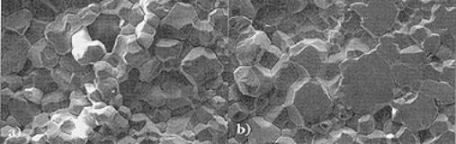
| | Figure 4. SEM images of an aluminium alloy that has been gallium etched to reveal its grain structure. | 3-D Grain Simulations To check the validity of grain microstructural measurement techniques and their relevance to 3-D grain structures, NPL has investigated techniques for 3-D grain simulation, e.g. aggregating computer generated polyhedra, Voronoi diagrams and cellular automata (CA). A Voronoi diagram (fig 5) is produced by placing random points in a 3-D virtual space and constructing planes between closest pairs of points. This produces a space-filling tessellation which resembles a grain structure. CA produce a ‘grain structure’ that is more realistic physically than the Voronoi method, but the technique has poorer resolution and is significantly slower Aggregation of polyhedra is most useful for materials like cermets. | 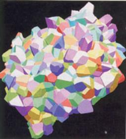
| | Figure 5. A slab of synthetic grains produced using a 3-dimensional Voronoi diagram. | Each of the techniques has a degree of randomness built into them and by regenerating simulation many times, statistics for many thousands of ‘grains’ can be produced. Also, because they are 3-D simulations, it is possible to measure a variety of parameters for each grain. They could be linear intercepts (1-D), sectional are (2-D), surface area (2-D) or volume (3-D). CA, which are related to Alan Turing's eponymous machines, can be thought of as small software robots that obey relatively simple rules defined by, in this case, the physics of grain growth from molten metal. |