In this interview, AZoM speaks to Dr. Dean Miller, Senior Scientist at TESCAN Group, about how plasma FIB-SEM can be used to accelerate multi-modal materials characterization.
Could you explain the fundamentals of focused ion beam scanning electron microscopy (FIB-SEM)?
FIB-SEM is based on a scanning electron microscope, which provides a focusable beam of electrons scanned onto a sample with electrostatic and electromagnetic lenses. As charged particles, the electrons interact very strongly with materials, with many signals emitted from the sample. These emitted signals offer us many ways to learn more about our sample.
Electrons scattered from the sample allow us to collect high-resolution images, yielding information about morphology and structure. Depending on the part of the electron spectrum used for imaging, we can also acquire compositional information, for instance, using backscattered electrons.
Other signals that emanate from the sample, such as characteristic X-rays that arise from the interaction of the incident electron with the atoms in the sample, can be measured spectroscopically to yield more information about composition.
The key characteristic of a FIB-SEM is the inclusion of a focused ion beam, another column that produces a focused beam of charged particles using ions instead of electrons. Like electrons, ions can be focused and directed to precise locations on the sample using electrostatic lenses. It is the beam’s focused nature that gives us powerful capabilities for nanoscale milling and patterning.
Ions are massive compared to electrons, allowing them to remove material through sputtering at the very specific locations we direct the beam. This gives us the capability to pattern and produces tiny objects.
The ions incident on the sample also induce the emission of electrons and secondary ions that we can use for imaging. This is useful because you can get very different contrast mechanisms with the ion beam compared to the electron beam. The ion beam can also be used for scattering and spectroscopy.
For example, by collecting and measuring secondary ions emitted from the sample using mass spectroscopy, we can learn more about our sample. The FIB itself provides powerful material characterization capabilities; however, the integration of FIB with SEM greatly expands the usefulness of both these approaches.
What are some of the common applications for FIB-SEM?
Cross-sectional imaging is one of the prime applications for FIB-SEM. We use the SEM to identify a very specific region, from which we carve into the sample using the ion beam to create a cross-section, before imaging or performing spectroscopy on the features revealed using both the electron and ion beams.
If we create a cross-section from both sides, we can extract a small piece of material for other measurements, for example, examination in a transmission electron microscope.
In addition, the FIB-SEM-based process can be applied to a wide variety of materials. It mitigates some of the challenges and limitations of preparing cross-sections of materials by more traditional or conventional methods.
Another use of FIB is for device fabrication and nanopatterning, using the focused ion beam to remove small amounts of material to create small devices. A gas injection system is also commonly integrated with FIB-SEMs, often used to deposit a protective layer or contacts at very precise locations.
Three-dimensional analysis is another core application of FIB-SEM. We can prepare a cross-section and then obtain information from it using imaging or spectroscopy. Because of the precise control offered by the FIB beam, we can repeat this process sequentially, collecting a series of images in a three-dimensional manner.
This ‘stack’ of images can be used to reconstruct and interrogate the three-dimensional structure of a material.
What are the limitations of FIB-SEM?
FIB-SEMs normally use a gallium-based FIB, but these do have some limitations. Researchers often want to analyze a larger area or volume of materials than can be effectively-prepared using a gallium FIB, leading to demand for a FIB that can mill larger volumes.
A second issue is gallium contamination. As a metal, gallium can react with many different materials, leading to changes in the microstructure or properties of the materials a Ga beam is directed upon, through implantation of Ga ions.
The third area of challenge for Ga FIB is amorphization and damage – which is intrinsic to the sputtering process using any ion beam. The incident ion displaces atoms; that is how we sputter material. Displaced atoms near the surface can exit the sample, but many displaced atoms remain in the material. If they do not return to their equilibrium positions, that leads to damage and, ultimately, amorphization. However, some other ion species, such as Xe, create damage in a shallower region than Ga.
Along with gallium-based FIB, there is also plasma FIB. What are the differences between these two techniques?
The strength of gallium FIBs is very small probes at relatively low currents. In contrast, a plasma FIB’s strength lies in relatively small probe size even at high currents.
A gallium-based FIB source typically consists of a sharp tungsten needle coated with a conformal layer of gallium. A voltage can be applied to extract Ga ions from the source, after which the electron-optical components of the column are used to form our focused ion beam.
With a sharp tip, a Ga FIB source is a point source, meaning we can form small probes without requiring a large demagnification. However, it is difficult to get high probe currents from such a small source because it has a small emission surface. As we try to extract more ions from this small source, more ions are emitted at higher divergence angles. Therefore, for higher currents, spherical aberrations significantly limit performance. As a consequence, the maximum probe current is typically in the range of 100 nanoamps for current state-of-the-art gallium-based FIBs.
In contrast, a plasma source consists of a small chamber in which we generate a plasma of ions. A gas such as Xe is introduced into the chamber and high-frequency radiation is used to strip electrons from the gas, creating the ions. Like the Ga source, voltage is used to extract the ions through a small hole in the chamber. This hole, while very small, is still relatively large compared to the small point source for a liquid metal ion Ga source.
The virtual source size for a gallium probe is on the order of tens of nanometers, while it is in the hundreds of microns for a plasma source. Because of this larger emission surface, we can extract a lot of ions from a plasma source, leading to more ions in our focused probe. That higher probe current, in the range of microamps, helps give us this capability to mill larger volumes very quickly. However, because we have a relatively large virtual source, we need large demagnification to form a small probe, and aberrations in the condenser lens system become a limiting factor when we try to form very small probes.
Aside from the high probe currents possible in a plasma FIB, another important aspect is the number of atoms that are sputtered per incident ion. For example, for a 30 kV incident ion on silicon, the Xe ion typical for a plasma FIB-SEM generates more sputtered atoms than a Ga ion. The details depend upon the target material and ion energy, but the difference in sputtered atoms can approach three times more for Xe ions than Ga ions.
The effect of higher current and a higher sputtering rate from a Xe plasma source lets us rapidly mill and remove large volumes of material. Depending on the target material, Xe plasma FIB milling can be 50 times faster than gallium FIB.
How does plasma FIB-SEM and gallium FIB-SEM compare when considering the damage done to samples? Can plasma FIB significantly outperform gallium FIB in this context?
One point of concern using FIB to study materials is amorphization and damage. Recent literature compares the amorphous damaged layer in silicon prepared using a gallium FIB against a xenon FIB. Under the conditions used in that study, the thickness of the amorphous layer produced on the sample resulting from ion irradiation was significantly lower with the xenon compared to gallium.
This effect can also be illustrated by simulations of the damage cascade produced by ions in simulations using a program named SRIM. Simulations show that xenon, as a larger ion, does not penetrate as deeply into the sample and the associated atomic displacements are more confined to the surface region, while the displacement cascade produced by Ga ions of the same energy extend much deeper into the sample.
There are two consequences to this. Firstly, we have more sputtering with a Xe ion because the displacement cascade is mostly confined to the surface. Secondly, the damage produced by the atomic displacements is also confined to the surface, leading to a shallower amorphous or damaged layer.
A lower accelerating voltage can reduce the depth of damage from ion milling, but the same difference between Xe ion impact and Ga ion impact is seen at lower voltages. The xenon penetrates less deeply and yields a higher sputtering rate and a shallower damage layer compared to Ga ions.
As a result of these effects, plasma FIB can overcome the challenges that gallium FIB faces, without significant compromise. We can address a large volume analysis, prepare samples without the influence of gallium contamination, and prepare the most delicate types of samples.
How can plasma FIB-SEM be used to accelerate materials characterization?
Plasma FIB can enhance capability for multi-modal characterization. There are a lot of different capabilities that we can integrate into the FIB-SEM instrument. Many of these are commonly integrated into SEMs, but when integrated into a FIB-SEM they expand our capabilities to understand materials because we can also shape, polish, or prepare the material with the FIB. This expanded capability really transforms the FIB-SEM into a versatile nanoscale laboratory for multi-modal analysis.
Examples of very powerful techniques that can be integrated into FIB-SEM include energy dispersive spectroscopy, electron backscatter diffraction, Raman, and TOF-SIMS.
When we direct electrons on a sample, many different interactions take place leading to many different signals. For example, the incident electrons can displace a core-shell electron from an atom in the sample. A higher level core electron can drop down to fill that shell, releasing a very specific, characteristic amount of energy in the form of an X-ray. In energy dispersive spectroscopy (EDS), a spectrometer measures the emission of X-rays coming from the sample.
The resulting spectrum will have peaks associated with this interaction of the incident electrons with the atoms in our sample, and the characteristic emission peaks will reveal a great deal about composition.
Electron backscatter diffraction (EBSD) relies on rescattering the incident beam in the sample leading to diffraction-based interaction with the crystallographic planes in the material. We capture that information as a Kikuchi pattern on a special detector before deconvoluting that pattern, which gives us important information about the crystallography of the sample.
In combination with the FIB for serial sectioning, this results in three-dimensional analytical information which can bring new insights into the material’s structure.
How this can be applied in materials research?
One example comes from research at the Ecole Polytechnique in Montreal to understand the nature of precipitates in high-strength steel and their connection to grain boundaries. This is an important use of these combined multi-modal techniques because we need to visualize the precipitates as well as the grains and grain boundaries. We use both EDS and EBSD to do this, with EDS revealing the precipitates based on their composition and EBSD revealing the grains based on their orientation.
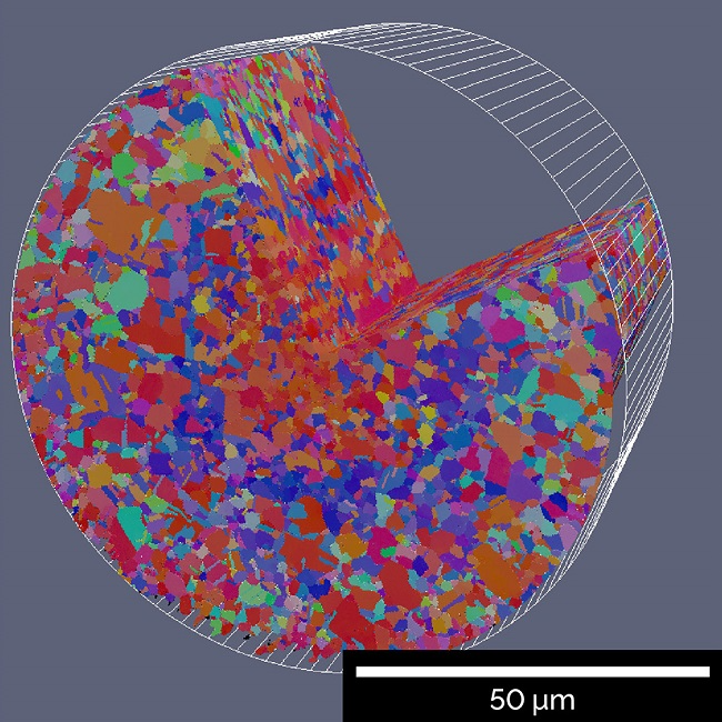
3D EBSD map of a 90 µm diameter cold-drawn copper wire
For novel materials prepared by additive manufacturing (3d printing), for example, it is essential to carry out such studies in three dimensions, and characterizing the appropriate volume of material is important in understanding their behavior. To have a good statistical representation of an ensemble of grains we need to know not only the grain size but also other important statistical parameters, such as their orientation and aspect ratio. These parameters can be measured using three-dimensional EBSD.
The plasma FIB facilitates this by allowing us to analyze a much larger, and therefore more statistically robust, volume of material. Different aspects of grain distribution can be obtained by other complementary methods, such as X-ray tomography, but the tremendous detail, spatial correlation, and the statistically significant volumes that are provided by the plasma FIB are vital for this sort of analysis.
What are the most recent trends in materials characterization?
Other capabilities for multi-modal characterization of materials include the integration of both Raman and time-of-flight secondary ion mass spectroscopy (TOF-SIMS) into the FIB-SEM.
FIB-SEM has been very helpful in research into improving the functionality of lithium-ion batteries, revealing cracking in cathode oxide particles that occurs during cycling, for example, that we suspect could be a problem. This has led researchers to develop models for loss of capacity based on the cracking and separation of particles.
The fantastic imaging from FIB-SEM provides information for such models about morphology and structure, but we also need information about what is happening with the lithium - we make use of Raman spectroscopy and the time-of-flight SIMS for this.
Raman spectroscopy provides information about the state of lithiation and disorder in these materials. Bands of peaks in the Raman spectra from these materials reflect the transition metal lithium bonds in the material, giving us information about the state of lithiation and bonding.
In the time-of-flight SIMS, we measure the secondary ions that are ejected from the sample as we sputter away material. We can measure the Li-ions directly with this technique, which gives us information about the local Li content. Because we scan the focused ion beam across a sample and measure the Li content at each point, we also acquire the spatial distribution of lithium - important information in understanding and validating these sorts of models.
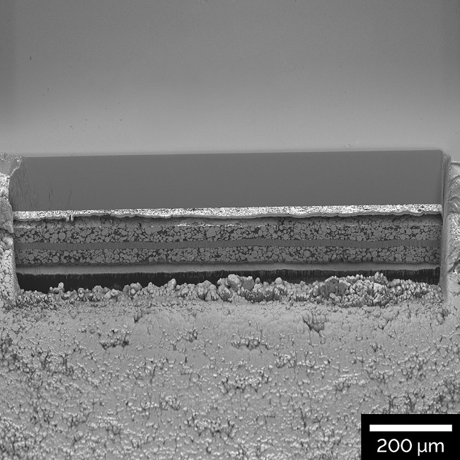
1 mm wide polished cross-section of a Li-ion battery electrode
Time-of-flight SIMS is an interesting integration for a FIB-SEM because it requires a primary ion beam to produce the secondary ions that we measure. In a FIB-SEM, we already have the primary focused ion beam available. When we want to integrate time-of-flight SIMS, we just add the time-of-flight detection system to the focused ion beam instrument. It is like simply adding an energy dispersive spectrometer to an SEM because, here, we already have the necessary primary focused ion beam.
The integration of Raman into the FIB-SEM is accomplished using a high precision stage, which translates the sample from a position under the electron and ion beams to a position beneath a Raman optics system, which is installed parallel to the SEM electron optical system.
In our case, we use a confocal Raman system that scans across the sample collecting spectra at every point. Those spectra are analyzed to identify similar features, revealing a particular phase. As we have this high precision stage, the structural information obtained by SEM and the spectral information revealed by Raman can be well-correlated in a Raman imaging and scanning electron (RISE) microscope image measurement.
Both TOF-SIMS and Raman data offer additional validation for the model described earlier as one mechanism of degradation in these lithium-ion battery materials, and this data and validation was made possible by multi-modal characterization in the FIB-SEM.
How does FIB-SEM perform in multi-scale characterizations?
We can use the FIB-SEM as a key component, not only for multi-modal characterizations but also for multi-scale characterizations.
For example, additive manufacturing brings in material research challenges that span a variety of length scales.
As we follow the additive manufacturing process through the deposition process to the thermal fusing process, it is important to understand how different parameters such as green pack and thermal processing influence the final properties of the densified material.
We need to explore these materials over a range of length scales, and developing a combination of capabilities to obtain this critical multi-scale information is still a work in progress. However, FIB-SEM is an essential component.
We use X-ray computer tomography to get three-dimensional information from a relatively large volume of the material. From this large volume analysis, we can identify regions within that volume that we want to understand in more detail at smaller length scales.
The plasma FIB is an ideal complement to the X-ray tomography because it allows us to explore the relatively larger volumes probed by x-ray tomography with resolution necessary for multi-scale imaging, or to use other multi-modal capabilities, even for volumes that would be difficult to access using a Ga-based FIB.
For example, using electron backscatter diffraction to assess the crystallographic orientation of grains in these materials would require relatively large cross-sections to obtain statistically significant data. Plasma FIB makes this sort of measurement possible.
In addition to understanding structures over larger volumes, it may also be important to understand surface contamination layers on the starting material, which would require analysis of the smallest, most detailed parts of the microstructure. Here too, plasma FIB-SEM plays a key role.
This complete workflow is enabled by a range of instruments, moving from X-ray tomography to plasma FIB-SEM.
Could you summarize the main benefits of plasma FIB-SEM?
A plasma FIB-SEM is a powerful means of exploring materials, going beyond what we can accomplish with a traditional gallium FIB. It allows us to produce large cross-sections and access volumes of materials much larger than is possible with a Ga FIB.
Sample damage is minimized because the larger ion Xe ion produces a shallower damage region than Ga, and gallium contamination is eliminated. Integrating additional characterization capabilities transforms the FIB-SEM instrument into a nanoscale laboratory for multi-modal characterization.
What FIB-SEM products does TESCAN offer?
TESCAN offers a wide range of FIB-SEM products for varying applications based upon the two different ion species we discussed above. In general, the Gallium ion source FIB-SEM products are typically for applications that need ultimate precision and the Xenon plasma FIB-SEM products enable access to larger volumes of material in shorter times frames.
TESCAN is a leading global supplier of SEM, FIB-SEM, and micro-CT solutions that are capable of imaging with both high resolution and high contrast - some solutions will even enable observation of dynamic events in real-time. The products are designed to be extremely versatile, allowing customization to provide valuable insights into a broad range of scientific disciplines. From materials science to cellular biology, semiconductors, and geology, our instruments help unlock the secrets of “how” and “why”. For more information, please visit www.TESCAN.com.
About Dean Miller, Ph.D.
 Dean Miller received his B.S. in Metallurgical Engineering and Ph.D. in Materials Science, both from the University of Illinois in Champaign-Urbana. He was a Senior Materials Scientist at Argonne National Laboratory for 30 years, including serving as Director for the Electron Microscopy Center at Argonne. His research focuses on the characterization of complex electronic oxides including advanced battery materials, magnetic oxides, and high-temperature superconductors with a particular emphasis on characterization by electron beam methods.
Disclaimer: The views expressed here are those of the interviewee and do not necessarily represent the views of AZoM.com Limited (T/A) AZoNetwork, the owner and operator of this website. This disclaimer forms part of the Terms and Conditions of use of this website.