New research in Chinese Physics Letters investigates the phenomena of superconductivity and charge density waves in a monolayer material grown on a graphene substrate.
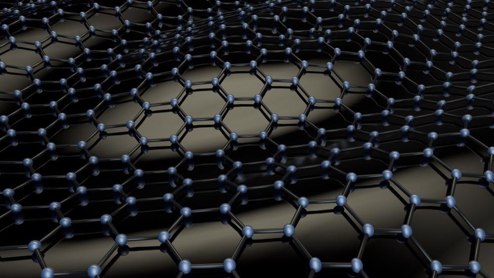
Study: Charge Density Wave and Electron-Phonon Interaction in Epitaxial Monolayer NbSe2 Films. Image Credit: 3DStach/Shutterstock.com
The discovery and development of monolayer superconductors have had significant implications for fundamental physics and for the development of new technologies.
While graphene has become a popular form of these materials, the fact that it lacks an electronic bandgap has spurred the search for other 2D materials with semiconductor properties.
Of these 2D materials, transition metal dichalcogenides (TMDs) are proving to be a promising alternative, exhibiting a variety of novel physics properties in electronics, photonics, and spintronics.
The key to understanding these materials is developing robust models of how their superconductivity and charge density wave (CDW) — an ordered quantum fluid of electrons in a linear chain compound or layered crystal — interact.
A new paper published in the journal Chinese Physics Letters looks at the interplay between superconductivity and CDW in Niobium Diselenide (NbSe2), a material that is an ideal way of testing both phenomena.
What Is Superconductivity?
The initial discovery of superconductivity occurred in 1911 when Dutch physicist Heike Kamerlingh Onnes and his team discovered that the electrical resistance of mercury goes to zero below 4.2 K (-269°C).
This led to the realization that below a certain critical temperature materials undergo a transition to a superconducting state. This results in the development of two important characteristics.
Firstly, the materials in question can no longer resist the movement of electrons that represents that passage of charge. At this point of zero resistance, the current can circulate in a material without any energy being dissipated.
The second significant characteristic of a superconducting state is that weak magnetic fields can’t penetrate a superconductor. Instead, the fields are held at the material’s surface. This field repulsion is known as the Meissner effect.
Both conventional physics and elementary quantum theory of the solid-state, — which treats the behavior of the electrons separately from that of the ions in the crystalline lattice — can’t adequately explain the superconducting state.
Doing this required a new microscopic theory of superconductivity, which suggested electrons form pairs in superconducting material through interaction with vibrations of the lattice — known as phonons. These so-called Cooper pairs move around inside the solid without friction, with the solid effectively considered a lattice of positive ions immersed in a cloud of electrons.
As an electron weaves through this lattice its ions are attracted by the electron’s negative charge and move slightly. This movement generates an electrically positive area with the knock-on effect of attracting another electron.
The sensitivity of the superconducting phase is a result of the fact that Cooper pairs can be easily broken up by thermal energy.
What is the Difference Between Superconductivity and Charge Density Waves?
Electrons in a CDW form a standing wave and collectively carry and current as they travel through a material en masse in a correlated way. This probably sounds a lot like the behavior of a superconductor.
The major difference between the two states is where electrons in Cooper pairs flow steadily through a superconductor. The electrons in CDW travel in fits and starts.
This can also be considered like a faucet through which water can flow freely, being turned off, but leaving a steady drip-drip-drip of water.
These periodic bumps in the flow of electrons in CDW are caused by a factor of quantum mechanics called particle-wave duality. This is most familiar when presented in the case of particles of light, photons.
Image Credit: Image Source Trading Ltd/Shutterstock.com
When photons travel they can be modeled as waves, but when they strike a surface their behavior is particle-like. This counterintuitive idea became even more revolutionary when researchers used the iconic double-slit experiment to discover the fact that electrons and other particles can also be modeled as waves. Thus they also have particle-wave duality.
For electrons, this phenomenon causes energy gaps between them and the “bumps” in charge that create CDWs.
In the 1930s, physicist Rudolf Peieris predicted CDW’s existence, arguing that a one-dimensional metal would be unstable to the formation of energy gaps at the Fermi wavevectors which reduce the energies of the filled electronic states.
These gaps form at what is known as the Peierls transition temperature when distortion of the periodic lattice of a one-dimensional crystal causes atomic positions to oscillate so that the perfect order of the 1-D crystal is broken.
This is all fine and well, but for superconducting and charge density wave phenomena to become useful, it is necessary to find materials that can reach these states without being lower to extremely cold temperatures.
That is where monolayer materials come in.
Investigating Superconductivity and Charge Density Waves in Niobium Diselenide
Niobium Diselenide (NbSe2) is a superconductor at temperatures below 7.2 K that also exhibits a CDW. When NbSe2 is created in a monolayer on a graphene substrate, it exhibits radically different properties than it does as a bulk material.
The transition temperatures in the monolayer 1H-NbSe2 grown on a graphene substrate are ∼3.0 K for superconductivity and ∼145 K for CDW. These temperatures are higher than those found in a bulk source of NbSe2, and for CDW this temperature is significantly higher.
The authors of this new study found that the two stable CDW states of monolayer NbSe2 can coexist on NbSe2/BLG surface at liquid-nitrogen temperature.
The team found that the charge transfer from the graphene substrates to the NbSe2 films grown on it influences the configurations of the Fermi surface — the surface which separates occupied electron energy states from unoccupied electron states at zero temperature.
This causes a 130 meV rise in the Fermi level —which determines the conductivity of different materials. This means superconductivity and CDW phases could be initiated at higher temperatures.
The authors conclude by suggesting that the electron-phonon coupling in monolayer NbSe2 dominates its CDW phase transition.
This could imply that the superconductivity and CDW behavior of monolayers of Niobium Diselenide could be influenced by the structure of the substrate upon which it is grown.
Reference
Xie. X., Lin. D., Zhu. L., et al, [2021], ‘Charge Density Wave and Electron-Phonon Interaction in Epitaxial Monolayer NbSe2 Films,’ Chinese Physics Letters. https://cpl.iphy.ac.cn/EN/0256-307X/current.shtml
Disclaimer: The views expressed here are those of the author expressed in their private capacity and do not necessarily represent the views of AZoM.com Limited T/A AZoNetwork the owner and operator of this website. This disclaimer forms part of the Terms and conditions of use of this website.