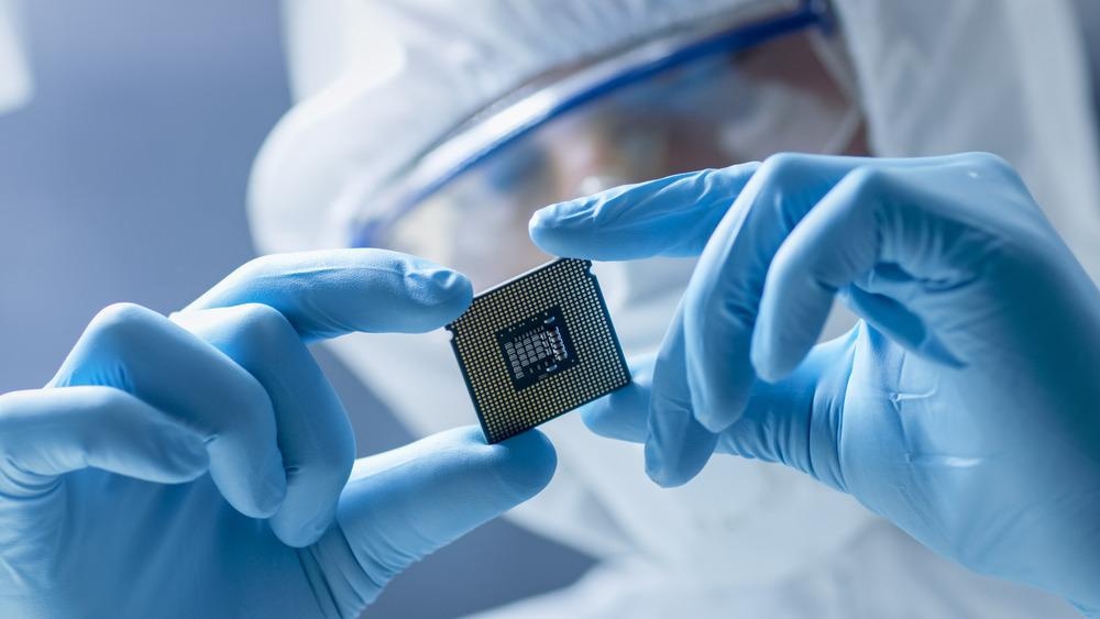
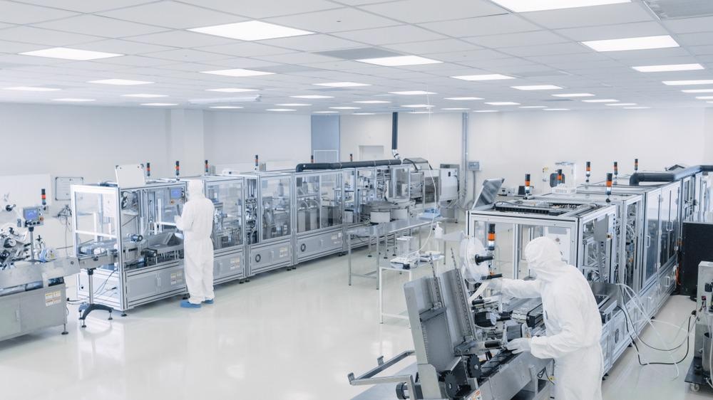
It would be hard to overstate the reliance of today’s society on semiconductors. From pacemakers to hypersonic missiles, smartphones to electric scooters, semiconductor materials are the basic building blocks of modern computation. With the annual production of devices that utilize these materials now surpassing 1 trillion, their effective recycling has never been more pertinent.

Image Credit: Gorodenkoff/Shutterstock.com
Semiconductor materials are those whose electrical conductivity falls between that of an insulator and a conductor. They may be elemental, such as silicon (Si) and germanium (Ge), or compounds, such as gallium arsenide (GaAs) or silicon carbide (SiC). Their immeasurable influence in progressing technology is due to the ability to manipulate their behavior by deliberately introducing impurities into their crystal structure, known as doping.
Semiconductor devices may be discrete in nature, such as transistors and diodes, or highly interconnected, where an array of electronic circuits are diffused into the surface of a thin slice of semiconductor material, called a wafer, to form an integrated circuit (IC).
How Are They Produced?
Whatever the end application of these devices, the chemical purity of the semiconductor material is paramount to their effective operation. Silicon, the most widely used of such materials since the 1950s, requires refining to a minimum purity of 99.9999% for use in solar cells and 99.9999999% for use in ICs.
This is usually achieved through a multi-step synthesis and purification process: carbothermal reduction of the naturally occurring oxide (SiO2, such as quartz), conversion into volatile silicon compound (such as trichlorosilane), distillation, decomposition to re-form elemental silicon in a higher purity, and zone refining (Barron, 2021). Only then, when impurity levels are in the parts per billion range, can the silicon be melted, doped, and undergo a crystal growth process (such as the Czochralski method) to finally achieve the desired single crystal material.
Other semiconductor raw materials must follow similarly complex synthesis and purification processes before they can be used in the fabrication of a semiconductor device.
Fabrication stages differ depending on the device in question; ICs for example, typically undergo masking (protecting selective areas of the wafer using a photoresist film), lithography (exposing the wafer to ultraviolet light to transfer a design onto the film), etching (removing the degraded film to reveal the intended pattern), ion implementation (doping the pattern by bombarding the material with ions), and metallization (creating the metallic interconnections for the individual devices).
The Need for a Circular Economy
The natural abundance of silicon, the economies of scale of semiconductor manufacturing, and the inadequate legislation concerned with e-waste are some of many factors which may conceal the very real need for circular economy approaches to be embedded within the semiconductor industry. The urgency of this is only recently becoming apparent amid the ongoing global chip shortage.
The Global E-waste Monitor revealed that of the 53.6 million metric tons of e-waste generated in 2019, only 17.4% was officially documented as properly collected and recycled. This represents a huge potential for sourcing secondary raw materials (including semiconductors), reducing emissions from the highly polluting synthesis and purification processes associated with virgin raw materials, and reducing harmful substances in landfill sites.
Recycling Methods
Recycling semiconductors is typically a complex, expensive, and polluting process, often supporting exploitative and hazardous labor practices in developing countries. But that is changing. Tremendous effort has been placed into developing sustainable and effective processes which can be used on a wide range of semiconductor devices.
Solar panels:
Over 90% of solar panels are based on crystalline silicon. Traditional recycling methods to extract this semiconductor relied upon highly toxic and corrosive chemicals such as hydrofluoric acid. Today, however, many greener alternatives are gaining popularity.
Bogust and Smith (2020) displayed that physical recycling methods, in this case comprising of the submersion in liquid nitrogen followed by pyrolysis and mechanical screening, enabled an 88% recovery rate of crystalline silicon particles from shredded solar panels. Rahman et al. (2021) showed that similar recovery rates were possible using environmentally friendly chemical methods, which could then be coupled with a ball milling process to give nano-silicon for use in battery electrodes.
Punathil et al. (2021) showed that sustainable and environmentally friendly recycling methods are also capable of extracting silicon of sufficient purity to be reused in new semiconductor devices.
ICs:
The complex composition of ICs means that recycling methods are particularly arduous and that methods that have been developed are usually concerned with the recovery of their precious metal components such as gold and silver.
However, semiconductor materials have been the focus of some recycling methods. Zhan et al., (2020) developed an environmentally friendly and efficient hydrothermal-buffering technique for the recycling of GaAs-based ICs, achieving gallium and arsenic recovery rates of 99.9 and 95.5% respectively. This work could prove even more relevant given the hypothesized uptake of GaAs-based ICs to meet the challenging demands of new technologies such as 5G and the Internet of Things.
Diodes:
The recycling of diodes, in particular light-emitting diodes (LEDs), is also proving an increasingly popular practice due to the critical raw materials they contain (such as gallium, indium, and rare earth elements), and the hazardous metals they can leach in landfill sites (such as lead and arsenic).

Image Credit: Gorodenkoff/Shutterstock.com
LEDs can contain GaAs, gallium nitride (GaN), or gallium phosphide (GaP) semiconductor materials depending on the desired color of light. Oliveira et al. (2021) showed that recycling strategies differed depending on which of these materials were present but highlighted the general superiority of a hydrometallurgy process (the extraction of metals based on reactions in an aqueous medium).
Transistors:
The semiconductors contained in discrete transistors are not currently recycled on a mass scale due to the packaging and size of these devices.
Last year, however, researchers at Duke University developed the first fully recyclable transistor. The printable device is fabricated from conductive (graphene), semiconductive (carbon nanotubes), and insulative (nano cellulose) inks. Recycling the carbon-based device is simple, requiring an ultrasonic bath and a centrifuge. The graphene and carbon nanotubes, both with recovery rates over 95%, can then be used again to print another device.
References and Further Reading
Barron, A., 2021. Chemistry of Electronic Materials. MiDAS Green Innovations. https://www.alibris.co.uk/Chemistry-of-Electronic-Materials-Andrew-Barron/book/49727639
Bogust, P. and Smith, Y., 2020. Physical Separation and Beneficiation of End-of-Life Photovoltaic Panel Materials: Utilizing Temperature Swings and Particle Shape. JOM, 72(7), pp.2615-2623. https://www.proquest.com/docview/2420726761
Dume, I., 2021. Carbon-based inks make first fully recyclable transistors. [online] Physics World. Available at: <https://www.sciencedaily.com/releases/2021/04/210426140908.htm>
Fort, V., Balde, C., Kuehr, R. and Bel, G., 2020. The Global E-waste Monitor 2020. Bonn: United Nations University/United Nations Institute for Training and Research. https://collections.unu.edu/view/UNU:7737
Oliveira, R., Benvenuti, J. and Espinosa, D., 2021. A review of the current progress in recycling technologies for gallium and rare earth elements from light-emitting diodes. Renewable and Sustainable Energy Reviews, 145, p.111090. https://ideas.repec.org/a/eee/rensus/v145y2021ics1364032121003786.html
Punathil, L., Mohanasundaram, K., Tamilselavan, K., Sathyamurthy, R. and Chamkha, A., 2021. Recovery of Pure Silicon and Other Materials from Disposed Solar Cells. International Journal of Photoenergy, 2021, pp.1-4. https://www.hindawi.com/journals/ijp/2021/5530213/
Rahman, M., Mateti, S., Sultana, I., Hou, C., Falin, A., Cizek, P., Glushenkov, A. and Chen, Y., 2021. End‐of‐Life Photovoltaic Recycled Silicon: A Sustainable Circular Materials Source for Electronic Industries. Advanced Energy and Sustainability Research, 2(11), p.2100081. https://onlinelibrary.wiley.com/doi/full/10.1002/aesr.202100081
Yoon, A., 2021. 5G and AIoT will need new semiconductor materials. [online] 5G Technology World. Available at: <https://www.5gtechnologyworld.com/5g-and-aiot-will-need-new-semiconductor-materials/>
Zhan, L., Zhang, Y., Ahmad, Z. and Xu, Z., 2020. Novel Recycle Technology for Recovering Gallium Arsenide from Scraped Integrated Circuits. ACS Sustainable Chemistry & Engineering, 8(7), pp.2874-2882. https://pubs.acs.org/doi/abs/10.1021/acssuschemeng.9b07006
Disclaimer: The views expressed here are those of the author expressed in their private capacity and do not necessarily represent the views of AZoM.com Limited T/A AZoNetwork the owner and operator of this website. This disclaimer forms part of the Terms and conditions of use of this website.