Thin film transistors (TFTs) are a kind of field-effect transistor in which the electrically conducting layer is formed by laying a thin film on the dielectric substrate or the supporting platform. TFTs are often employed in display applications, particularly liquid crystal displays (LCDs).
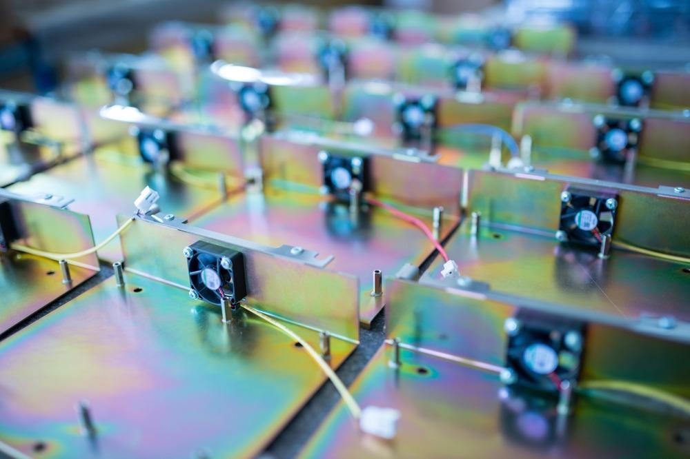
Image Credit: YouraPechkin/Shutterstock.com
What are Thin-Film Transistors and How do They Operate?
Thin-film transistors (TFTs) are a kind of metal-oxide-semiconductor field-effect transistor (MOSFET) made by covering an insulating substrate with an activated semiconductor layer, metallic connections, and a dielectric layer. As the need for smart and flexible electronic devices and integrated systems grows, novel materials with great mobility and low production costs become more important.
Printable TFTs are a significant printed electronics application. Channel semiconducting materials have a considerable impact on the performance of printed TFTs. In comparison to organic semiconductors, semiconducting single-walled carbon nanotubes (sc-SWCNTs) have much higher charge movement. Sc-SWCNTs are also more physically and chemically stable.
A liquid crystal display (LCD), which includes a transistor for each pixel and is prevalent in the notebook and portable computers, is a display screen produced utilizing thin-film transistor (TFT) technology. Because each pixel has a transistor, the current that drives pixel lighting may be lower and hence turned on and off more rapidly.
Materials used for Fabrication of TFTs
Thin-film transistors may be made from a variety of semiconductor materials, namely silicon, cadmium selenide, and zinc oxide. Recent technological advances have enabled researchers to explore organic resources to make TFTs. Organic transistors or organic TFTs are thin-film transistors built from organic compounds.
The light must be able to travel through the base material to reach the observer in a flat-panel display. A translucent silicon wafer is insufficient for these emitter screens. Because glass is very clear and suitable for typical semiconductor manufacturing procedures, it is the most widely utilized starting substrate. Because glass is not a semiconductor like silicon, a small coating of silicon is deposited on top, and transistors are built utilizing this thin coating.
Applications of Thin-Film Transistors
A TFT, as a typical fundamental electronic device, has attracted increased interest due to a variety of uses not just for panel displays but also for different types of sensors and as a core component of translucent and/or adaptable electronic components.
Thin film transistors are often found in laptops, flat-panel displays, video game systems, and cell phones. TFT technology has transformed video systems, allowing for greater size flat displays.
This innovation is used in a variety of contemporary gadgets, including LCD TVs, LCD monitors, laptop computers, cell phones, and tablets. TFT technology is also being researched in a variety of other fields, including X-ray sensing, optoelectronics, sensing applications, and biochemical detection.
Thin-Film Transistors: Advantages and Limitations
Thin-film transistors provide several benefits, including cheap cost, low power consumption, quicker reaction time, and higher response rate. TFT LCD screens are particularly handy due to their low energy consumption; conserving energy is a top goal in today's society to minimize greenhouse gas emissions and secure a brighter future.
TFTs also increase the capability of displaying dynamic images. TFT displays provide superior color saturation, lower power usage, and better contrast as compared to standard displays. TFT display pictures are free of flicker and have little to no image distortion since they do not depend on the processing of the beam of electrons.
TFT LCD is not without its drawbacks. Because of the nature of the design, TFT LCDs may cost somewhat more than standard monochrome displays. Thin-film transistor market growth is also constrained by constraints such as poor color accuracy, quality fluctuation, and depth of field. However, it is believed that future technical advancements would result in major increases in viewing quality.
Recent Studies and Advancements
Thin-film transistor (TFT) platform that can be used with plastic substrates is still in its initial phases of development. There is a lot of space for advancement in ultra-low temperature poly-Si TFT fabrication. For high-performance, active-matrix LCD applications, high mobility, low leakage current flow, and threshold values are especially desired.
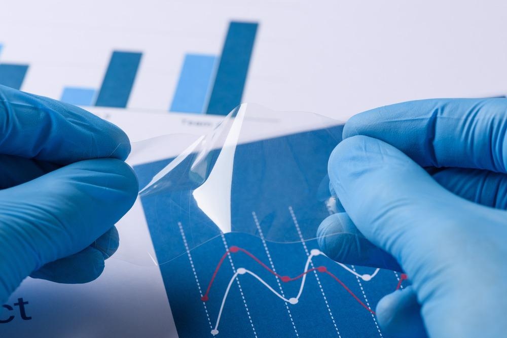
Image Credit: nevodka/Shutterstock.com
The TFT team at the University of California Berkley is working on an ultra-low-temperature (100oC) manufacturing technique that would be appropriate for flexible plastic substrates. The objective is to develop polycrystalline-silicon (poly-Si) thin-film transistors (TFTs) with current-driving capabilities significantly superior to that of traditional amorphous silicon TFTs now used in high-performance LCDs.
Physical vapor deposition is often employed in the production of thin-film transistors owing to the necessity for low temperatures and a very clean environment. The researchers at Utrecht University are looking at hot wire (catalytic) chemical vapor deposition (HWCVD) as a deposition process for creating unique TFTs that have a high capability to overcome the needs of a contemporary display.
Future Outlook
As conventional displays continue to dominate the global TV industry, TFT LCDs have lots of room to develop. As a result, screens will be the primary driving factor in the evolution of TFT technology shortly. Even though the quality of today's TFT LCDs is adequate for most users, manufacturing costs may be decreased further.
The present trends of lowering masking procedures, reducing each unit production time, broadening process windows, and removing contamination sources are projected to continue. The expense, productivity, and durability of the large-area array technique will decide whether or not an oxide TFT can substitute a silicon-based TFT in LCD applications.
More from AZoM: Measuring the Dielectric Constant in Thin Films
References and Further Reading
Duan, X. (2020). Nanowire Thin Films for Flexible Microelectronics. In X. Duan, Encyclopedia of Materials: Science and Technology. Elsevier.
Guo, X., Han, L., & Houa, X. (2021). Insights into the device structure, processing, and material design for an organic thin-film transistor towards functional circuit integration. Materials Chemistry Frontiers. Available at :https://doi.org/10.1039/D1QM00334H
Jr., A. H., Dizon, J. R., Valino, A. D., & Advincula, R. C. (2022). Advancing flexible electronics and additive manufacturing. Japanese Journal of Applied Physics. Available at: https://iopscience.iop.org/article/10.35848/1347-4065/ac621a/meta
Nauticomp. (2021, May 26). What Are Some Pros and Cons of TFT Displays? Available at: https://nauticomp.com/what-are-some-pros-and-cons-of-tft-displays/
Pandey, M., Rashiku, M., & Bhattacharya, S. (2021). Recent progress in the development of printed electronic devices. In M. Pandey, M. Rashiku, & S. Bhattacharya, Chemical Solution Synthesis for Materials Design and Thin Film Device Applications. Elsevier. Available at :https://doi.org/10.1016/B978-0-12-819718-9.00008-X
Disclaimer: The views expressed here are those of the author expressed in their private capacity and do not necessarily represent the views of AZoM.com Limited T/A AZoNetwork the owner and operator of this website. This disclaimer forms part of the Terms and conditions of use of this website.