To ensure compliance with industrial quality standards and specifications, semiconductor testing is vital. Due to inevitable fabrication flaws, testing is necessary to ensure fault-free semiconductor chips. This article covers the basics of semiconductor testing, equipment, working principles, and market trends.
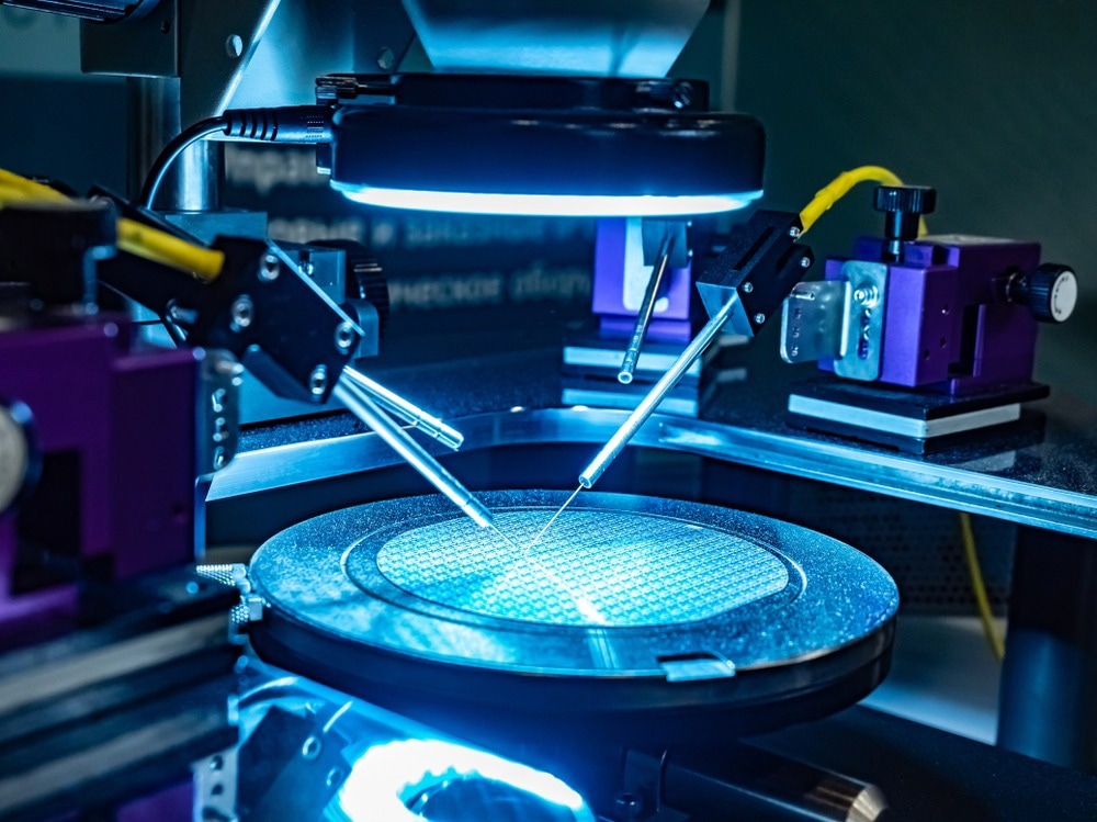
Image Credit: FOTOGRIN/Shutterstock.com
Semiconductor IC Testing
During standardized chip fabrication, integrate circuit (IC) testing is conducted repeatedly to inspect the chips once they are manufactured. IC testing begins with wafer penetration before etched wafers are dissected and turned into prepacked chips. Many of the flaws in today's procedures can only be identified and isolated via the test results. Tests are the gates that control time-to-yield, time-to-market, and time-to-quality.
Boolean testers, memory testers, and analog testers are the three broad categories into which testers fall. Wafer inspection and packaging testing are included in these tests. When testing wafers, a prober and a sensor chip are used; during packages inspection, a controller, a testing socket, and a tester are used.
Types of IC Testing
Integrated semiconductor circuit testing is broadly classified into three types: functional tests, structural tests, and parametric tests.
During a functional test, the chip is put through all the multiple operational functions it intends to perform. A structural test puts the product through an activity that will highlight any flaws that could be present as a result of manufacturing errors. Specific parameters, including current and voltage levels, will be determined through a parametric test. To determine a device's particular electronic characteristics, parametric testing is performed.
Introduction to Automated Test Equipment (ATE)
Automated test equipment (ATE) is a testing tool created to run one test, or a series of tests, on one or more devices simultaneously. Testing of semiconductors, equipment, and electronics is one of the many ATE tester applications.
An ATE system can be visualized as a box containing extremely complex electronic metering and stimulus devices that are managed by a PC or workstation. This processor regulates the transmission of data to the equipment for configuration and the production of stimulus signals. Additionally, it gathers and evaluates the information recorded and evaluated by the ATE system's hardware.
How Do Different Components Work in ATE?
Hardware, software, test tools, signal generators, and testing probes or handlers are the five essential parts of an automated test system.
Within the ATE field, the bit of software that regulates the data flow of stimuli and statistics is referred to as a "Testing Program" or "Application Program." Each automation testing device type, as well as each microchip to be evaluated, requires a unique test program to be created.
Additionally, an ATE network is comprised of an electronic interface known as the "Device Under Test" that enables interaction with the device being tested (DUT). A positioning tool is utilized in mass manufacturing to autonomously link the DUT to the ATE. This positioning tool for integrated gadgets is referred to as a handler. A "prober" is used to handle semiconductor wafers.
Advantages of ATE
By modernizing and optimizing testing tools, methods, and operations that were previously manual, ATE systems reduce testing times and generate significant financial savings for businesses. By removing wildly inconsistent operator intervention, automation assures uniformity in test and cycle times.
Why is Transistor Self-Heating a Major Problem?
Transistor self-heating is a major problem that is being researched extensively as per the study published in the 2021 IEEE 39th VLSI Test Symposium (VTS). Self-heating has a significant impact on-chip performance, including component dispersion deterioration, negative output permeability, threshold voltage change, and microchip reliability.

Image Credit: aslysun/Shutterstock.com
To begin with, conventional on-chip heat sensors/diodes only monitor the silicon die level and so cannot monitor or perceive self-heating because the energy generated is contained within transistors and cannot reach the silicon wafer, at which on-chip temperature sensors can detect it.
However, existing on-chip delay detectors will also fail to perceive self-heating because, amidst the high temperature produced by self-heating, the respective effect on the stimulated delay boost in logic gates may be limited and within the acceptable spectrum associated with traditional process fluctuation.
Novel Non-Destructive Semiconductor Testing
The 2022 Moscow Workshop on Electronic and Networking Technologies (MWENT) presented a study focused on a confocal infrared microscope that is being designed for the non-destructive testing of semiconductor structures. The laser scanning confocal infrared microscope (LSCIRM) in development is based on infrared microscopy (IRM) and confocal laser scanning microscopy concepts (CLSM).
Unlike existing semiconductor research methodologies, the LSCIRM will allow the identification and evaluation of faults, gaps, or foreign material entrapment not only on the exterior but also within the interior structure. LSCIRM does not necessitate any particular environmental parameters during research, such as a sealed chamber.
LSCIRM can also be utilized for reverse engineering, probing for mechanical backdoors, and, as a result, counterfeit detection. The basic architecture of LSCIRM allows it to be paired with a variety of laser sources. It enables the conduct of various radiation studies on ICs, as well as the use of analytical non-destructive testing procedures.
Future Market Trends
A market research report published in Fortune Business Insights presents a thorough market trend analysis of the semiconductor testing industry. The worldwide semiconductor fabrication and testing operations market is expected to increase at a CAGR of 5.5 percent from $31.86 billion in 2021 to USD 46.24 billion by 2028.
The high-end semiconductor testing and assembly industry necessitate a large capital expenditure to produce pricey equipment. The growing requirement for reduced temperature ratings necessitates the use of innovative packaging techniques. These investments are well-known among market players. However, small and medium-sized businesses find it challenging to provide high-end services, stifling worldwide market growth.
In short, semiconductor testing equipment is fabricated specifically for the intended testing procedure. However, much research is still needed to overcome shortcomings and pave the way for the rapid commercialization of wireless testing equipment.
More from AZoM: A to Z of Electromagnetic Shielding
References and Further Reading
Daniel, B., 2021. What is Automated Test Equipment?. [Online] Available at: https://www.trentonsystems.com/blog/automatic-test-equipment-overview#:~:text=its%20proper%20functionality.-,What%20are%20the%20components%20of%20an%20ATE%20system%3F,and%20test%20probes%20or%20handlers.
Fortune Business Insight, 2022. Semiconductor Assembly and Test Sats Market. [Online] Available at: https://www.fortunebusinessinsights.com/semiconductor-assembly-and-test-services-sats-market-106429
MJC, 2022. What is semiconductor test equipment (IC tester)?. [Online] Available at: https://www.twmjc.com.tw/technical_column-detail/56/
Prakash O. et. al. (2021). Transistor Self-Heating: The Rising Challenge for Semiconductor Testing. 2021 IEEE 39th VLSI Test Symposium (VTS): Available at: https://www.doi.org/10.1109/VTS50974.2021.9441002
Ukolov, D., Baluev, A., Gromova, P., Pechenkin, A., & Mozhaev, R. (2022, June). Laser scanning confocal IR microscopy for non-destructive testing of semiconductors. In 2022 Moscow Workshop on Electronic and Networking Technologies (MWENT) (pp. 1-3). IEEE. Available at: https:www.doi.org/10.1109/MWENT55238.2022.9802329
Disclaimer: The views expressed here are those of the author expressed in their private capacity and do not necessarily represent the views of AZoM.com Limited T/A AZoNetwork the owner and operator of this website. This disclaimer forms part of the Terms and conditions of use of this website.