Sponsored by Xenocs SASReviewed by Louis CastelMar 29 2023
Organic semiconductors (OSCs) are promising advanced materials due to their numerous attractive properties, such as their processability (low-temperature processing, low-cost production) and their lightweight and mechanical flexibility.1
They have exciting prospects for utilization in many applications, such as organic transistors, organic light-emitting diodes, sensors and biosensors, thin film batteries, or organic photovoltaics (OPVs).2 However, intrinsic disadvantages currently prohibit them from being utilized on a larger scale.
For example, despite organic solar cells achieving efficiencies similar to their inorganic (silicon) counterparts (greater than 18%), the manufacturing processes for this state-of-the-art photovoltaics are not suitable for large-scale production.
Utilizing methods of mass production, like roll-to-roll coating, materials of lesser performance are attained (5-10% efficiency).3 Enhancing the current understanding of these shortcomings and creating new production methods is a vital step that has been attracting growing interest from the scientific community.
A group of researchers from the Jülich Centre for Neutron Science (JCNS) at Heinz Maier-Leibnitz Zentrum (MLZ) and the Technical University of Denmark, the Deutsches Elektronen-Synchrotron (DESY), proposed a technique for manipulating the morphology (and implicitly the physical properties) of one such organic semiconductor with the use of visible light during roll-to-roll slot-die coating.3
Their research was centered on the conjugated polymer poly(3-hexylth-iophene) (P3HT) that is frequently utilized as an electron donor material in donor-acceptor heterojunctions for OPVs.
Generally, conjugated polymers, and specifically P3HT thin films, display changes in their morphology when illuminated with visible light. These structural changes then stimulate modifications of the physical and electric properties of the films.
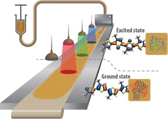
Figure 1. Illustration of the manufacturing method where poly(3-hexylth-iophene) is slot-die coated on a moving substrate in dark or while illuminated with red, green or blue light. Image Credit: Adv. Funct. Mater., 2023, DOI: 10.1002/adfm.202212835
As displayed in Figure 1, P3HT will shift from a ground state to an excited state during coating with visible light. The main structural difference between these two states is represented by the value of the dihedral angles between neighboring thiophene rings.
While the ground state exhibits twisted geometries, the excited states are completely planar. To examine these morphological changes caused by four different light treatments (with energies both above and below the excitation energy levels of P3HT), the researchers conducted grazing incidence wide-angle X-Ray scattering (GIWAXS) measurements.
Grazing incidence X-Ray scattering measurements have contributed significantly to gaining an understanding of the morphology of active materials and thin film layers used in OPVs.4
Light-Induced Changes in the Morphology of Organic Semiconductors as Studied by GIWAXS
GIWAXS is a very useful method that is generally utilized to establish the alignment of the polymer chains (backbone orientation) in thin films that have been deposited onto substrates. Figure 2(a) shows the typical patterns that may be observed in 2D GIWAXS for the coexistence of face-on and edge-on orientation motifs.
For the edge-on orientation, the chain backbone is positioned parallel to the substrate, together with the π-π stacking direction, while the side chains are aligned perpendicularly to the substrate.
Conversely, for the face-on orientation, the π-π stack is perpendicular to the substrate, and both the chain backbone and side chains are aligned in the plane of the substrate. These distinct orientations have an effect on the electrical properties and need to be considered when designing and optimizing P3HT-based devices.4
For example, an extract of two-dimensional GIWAXS patterns documented as part of this study is depicted in Figures 2(b,c), showing that the P3HT displays a predominantly edge-on orientation with some degree of orientation distribution.3
![(a) Typical GIWAXS scattering pattern that can be observed from a combination of edge-on and face-on phases. Note that the color code indicates the origin of each pattern. Image adapted from Ref. [5] (b, c) GIWAXS data recorded on P3HT thin films deposited on silicon substrate and treated with blue light or untreated.](https://www.azom.com/images/Article_Images/ImageForArticle_22559_16797205097817436.jpg)
Figure 2. (a) Typical GIWAXS scattering pattern that can be observed from a combination of edge-on and face-on phases. Note that the color code indicates the origin of each pattern. Image adapted from Ref. [5] (b, c) GIWAXS data recorded on P3HT thin films deposited on silicon substrate and treated with blue light or untreated. Image Credit: Adv. Funct. Mater., 2023, DOI: 10.1002/adfm.202212835.
Here, both in-plane and out-of-plane lamellar (100) reflections have been analyzed as a function of applied light treatment. As depicted in Figure 3(a), samples exposed to blue and green light displayed an intensity reduced by half and a maximum intensity at lower qz values compared to the ones exposed to dark or red light.
These observations demonstrate that treatment of the P3HT films with a blue and green light will cause a rise in the real space lamellar packing distance, in addition to a reduction of both the edge-on oriented aggregates and the crystallinity.
This reduction in crystallinity was also verified by atomic force microscopy measurements (AFM) which revealed a surface roughness reduction in samples treated with blue and green light.
When looking at the in-plane component, however, the opposite trend is observed (see Figure 3 (b)). The measured intensities rise significantly (approximately four-fold) in films treated with blue and green light. This suggests a severe increase in the fraction of aggregates oriented face-on with respect to the substrate.
The distribution of lamellar stacking orientations, with respect to the substrate, may also be calculated from GIWAXS measurements. As presented in Figure 3(c), photoexcitation with blue and green light causes a considerably higher fraction of face-on polymer chains.
Contrastingly, dark and red light treatments produce predominantly edge-on oriented crystallites.
When analyzing the real space in-plane lamellar stacking distance, calculated from GIWAXS measurements (shown in Figure 3 (d)), it becomes clear that less efficient packing (larger lamellar stacking distance) is obtained when samples are exposed to green or blue light.
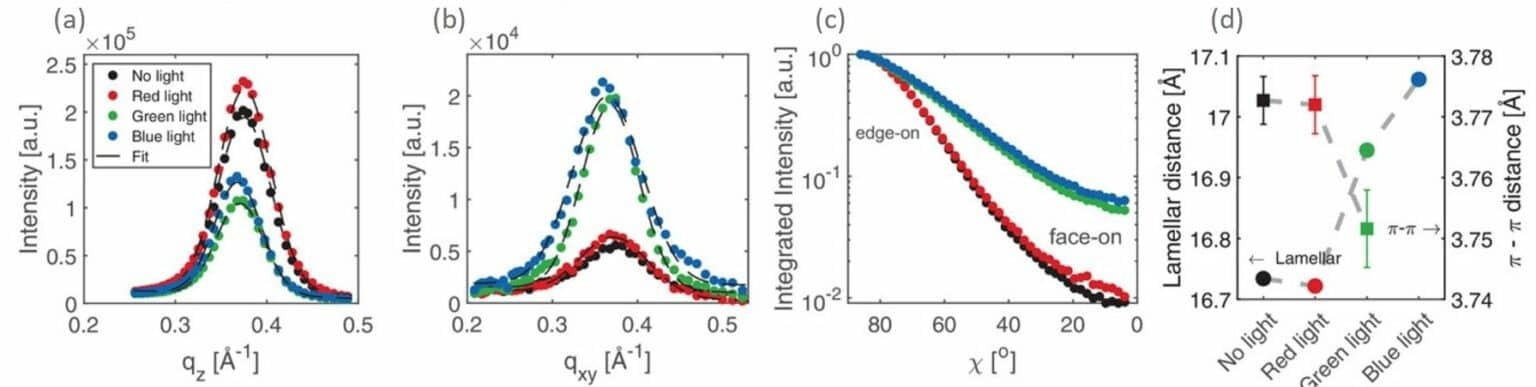
Figure 3. Line integration of (a) out-of-plane and (b) in-plane lamellar (100) peak and Gaussian fit. (c) Integrated lamellar signal showing the orientation of the polymer planes with respect to the substrate: 90o corresponds to out-of-plane orientation (edge-on) while 0o corresponds to in-plane orientation (face-on). (d) Out-of-plane lamellar distances and in-plane π- π stacking distances for each light treatment. Note that no in-plane π- π stacking distance was observed following the blue light treatment. Image Credit: Adv. Funct. Mater., 2023, DOI: 10.1002/adfm.202212835.
Influence of Morphology on the Electrical Properties of Organic Semiconductors
Regarding conductivity, both groups of light treatment generate considerably different properties. While dark and red light treatments promote in-plane photo conductivity, blue and green light treatments lead to mainly out-of-plane charge transport, as shown in Figure 4.
Polymer conductance is known to be limited by the inter-chain transport, and this can be directly correlated with the change of morphology from edge-on to face-on induced by the two types of light treatment, as revealed by GIWAXS.
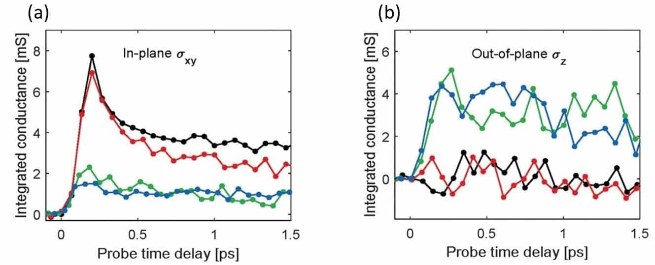
Figure 4. Spectrally integrated (a) in-plane and (b) out-of-plane sheet conductivity extracted from full 2D time-resolved terahertz spectroscopy (TRTS) scans at normal incidence and at 45o incidence respectively. Image Credit: Adv. Funct. Mater., 2023, DOI: 10.1002/adfm.202212835.
For organic photovoltaic applications utilizing P3HT thin films, it is necessary to carefully consider the orientation of P3HT crystallites regarding the reference plane (bottom electrode) represented by the substrate surface.
The anisotropic conductivity of P3HT is greater along the backbone chains and the π-π stacking in the edge-on configuration, resulting in higher efficiency for charge transport parallel to the substrate surface.
Conversely, the edge-on orientation with perpendicular staking will be impaired by a decreased exchange of charge carriers with the electrodes. Resultingly, the face-on orientation is favored for OPV applications as it enables a better exchange of charge carriers with the electrodes.
Conclusions
This study reveals that the thin film morphology of P3HT can be adapted by the application of different light treatments during deposition. It shows that manipulation of the packing behavior of P3HT in this manner can be utilized as a tool to realize the desired electric performance of these organic semiconductors thin films.
GIWAXS was proven to be an effective tool for studying the structural differences of thin films subjected to different photoexcitation treatments, which can be correlated with the various functions.
Most notably, it demonstrated that the application of blue or green light treatment during roll-to-roll slot-die coating produces primarily face-on oriented crystallites, a favorable orientation for OPV applications since it enables the better exchange of charge carriers with the electrodes.
Acknowledgments
The research detailed in this article was originally published in the following article: Sørensen, M. K., Gertsen, A. S., Fornari, R. P., Zhou, B., Zhang, X., Jepsen, P. U., … & Andreasen, J. W. (2023). Manipulating organic semiconductor morphology with visible light. Advanced Functional Materials, 2212835.
References
- Myers, J. D., & Xue, J. (2012). Organic semiconductors and their applications in photovoltaic devices. Polymer Reviews, 52(1), pp. 1-37.
- Martín-Palma, R. J., & Martínez-Duart, J. (2017). Nanotechnology for microelectronics and photonics. Elsevier.
- Sørensen, M. K., Gertsen, A. S., Fornari, R. P., Zhou, B., Zhang, X., Jepsen, P. U., Stanzani, E., Yun, S., Fernández Castro, M., Schwartzkopf, M. & Andreasen, J. W. (2023). Manipulating organic semiconductor morphology with visible light. Advanced Functional Materials, p. 2212835.
- Müller‐Buschbaum, P. (2014). The active layer morphology of organic solar cells probed with grazing incidence scattering techniques. Advanced materials, 26(46), p. 7692-7709.
- Osaka, I., & Takimiya, K. (2015). Backbone orientation in semiconducting polymers. Polymer, 59, A1-A15.

This information has been sourced, reviewed and adapted from materials provided by Xenocs.
For more information on this source, please visit Xenocs.