ScAlMgO4 (SCAM) crystalline substrates are attracting interest as a possible alternative to sapphire and silicon carbide. The article discusses the utilization of SCAM substrates for nitride semiconductors.
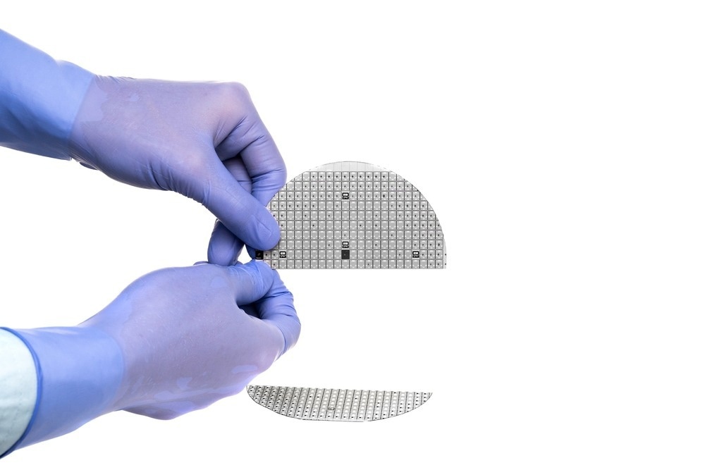
Image Credit: Slava73/Shutterstock.com
Nitride semiconductors have become a fundamental component of contemporary digital equipment, such as light-emitting diodes (LEDs), power systems, and radio transmission. Due to their potential uses in optoelectronics such as blue-, violet-, and ultraviolet (UV)-light emitting devices as well as elevated-temperature, high-frequency, and high-power electronic equipment, interest in GaN and ZnO as wide-band-gap semiconductors has increased.
A Brief Overview of SCAM Substrate Properties
SCAM crystal substrates are composed of a combination of scandium (Sc), aluminum (Al), magnesium (Mg), and oxygen (O2). The cubic crystalline lattice of SCAM has a lattice parameter of 8.086Å. The low coefficient of thermal expansion of the SCAM substrate makes it an excellent substrate for the development of nitride semiconductors. Furthermore, SCAM's excellent thermal conductivity aids in the dissipation of the heat created by nitride semiconductors during functioning. SCAM also possesses outstanding mechanical qualities, including superior elastic modulus and rigidity.
Traditional Substrates for Semiconductors
Nitride microelectronics have developed differently from traditional semiconductors such as Si and GaAs, as even the most typical nitride semiconductor, GaN, lacks a bulk substrate. LEDs are typically produced on sapphire substrates with a lattice mismatch to GaN of 13.8%. Using SiC substrates with greater thermal conductance than sapphire, HEMTs for mobile phone base stations have been manufactured.
Recent sample shipments of GaN wafers manufactured using the ammonothermal technique have commenced. These wafers have a dislocation density of only 102-3/cm2. On the other hand, exceptionally dense GaN films have been produced on foreign materials such as GaAs and sapphire using halide vapor phase epitaxy (HVPE), whose growth rate is approximately one order of magnitude greater than that of the ammonothermal approach.
Why is ScAlMgO4 a Better Substrate Than its Counterparts?
Sapphire's strong thermal conductivity and low coefficient of thermal expansion make it an excellent material for the formation of nitride semiconductors. Unfortunately, sapphire's limited tensile characteristics prevent it from being utilized in high-power and high-temperature applications. Another common substrate, silicon carbide (SiC), is more costly than sapphire and has a greater dislocation density, which might impact the efficiency of nitride semiconductor devices.
Compared to sapphire and SiC, ScAlMgO4 has a lower thermal expansion coefficient, which minimizes the stress on the nitride dielectric layers during growth. It also has a superior thermal conductivity than sapphire, allowing it to dissipate heat more efficiently. ScAlMgO4 is preferable to sapphire and GaAs as a foreign substrate for nitride heteroepitaxial film deposition mainly due to its 1.8% lattice misfit.
Industrial Utilization
The capacity to produce high-quality epitaxial layers is one of the primary benefits of utilizing SCAM crystal substrates for nitride semiconductor growth. The electrical and optical characteristics of a nitride semiconductor device are determined by its epitaxial layers, which are crucial to the device's performance. For blue and green LEDs, high-quality epitaxial layers of gallium nitride (GaN) are grown on Silicon crystal substrates. Using SCAM crystal substrates, nitride semiconductor layers for laser diodes have also been grown.
Power electronics is another possible use area for SCAM crystal substrates. In several applications, including electric cars, renewable energy systems, and industrial equipment, the flow of electrical power is regulated by power electronic components such as transistors and diodes. Due to their high breakdown voltage and strong thermal conductivity, nitride semiconductors are desirable for power electronics that are manufactured via the utilization of SCAM substrates.
How is ScAlMgO4 Substrate Fabricated Commercially?
Typically, SCAM crystal substrates are created using the Czochralski (CZ) process, a popular technique for generating single-crystal substances. In the CZ process, a seed crystal is dipped into the composite material's molten state and then gently extracted while spinning. As the seed crystal is extracted, the molten material hardens into a single crystal. The procedure is continued until a huge single crystal is produced, which is subsequently cut into wafers for use as substrates.
Latest Research
In the latest research published in the journal Crystals, the features of SCAM in terms of lattice constant, the coefficient of thermal expansion, and thermal transfer are thoroughly described by the researchers.
The fabricated SCAM crystal for the study had a diameter of more than 60 cm. Yet, the region of uniform composition measured was over 2 inches in circumference.
Using X-ray diffraction (XRD) at high temperatures, the thermal expansion coefficient (TEC) of a (0001)-oriented SCAM single crystal was determined. The contour of the recorded rocking curve has a single, sharp, symmetrical apex. By rocking curve results and the absence of misoriented sub-grains in the X-ray irradiated area, the outcomes showed that the SCAM-grown single crystal had outstanding crystal perfection, the same as a single crystal Si.
At room temperature, a and c-axes lattice parameters found were 0.32426 nm and 2.50850 nm. No phase transition-related irregularities were found in the temperature dependences of either lattice parameter. It was discovered that the thermal expansion coefficients of the a- and c-axes increased linearly with temperature.
At room temperature, the SCAM and Cp values were 0.014 ± 0.002 cm2 and 0.86 ± 0.03 J/g K (or 138 ± 5 J/mol K), respectively. This number was in satisfactory correlation with the 128.6 J/mol K derived using Kopp's equation, which illustrates the linear connection between a solid's heat capacity and its constituent composition. As one of the fundamental features of crystals, the Raman scattering spectroscopic data on lattice vibration modes confirmed the existence of crystal symmetry.
SCAM is transparent throughout a broad spectrum of wavelengths, from ultraviolet to mid-infrared. Therefore, SCAM is appropriate for use as a platform for nitride electronics such as LEDs and solar cells.
More from AZoM: Density Functional Theory Applied to Optoelectronical Properties of Graphene
References and Further Reading
Shtepliuk, I. et. al. (2021). Temperature-dependent photoluminescence of ZnO thin films grown on off-axis SiC substrates by APMOCVD. Materials, 14(4), 1035. Available at: https://doi.org/10.3390%2Fma14041035
Matsuoka T. et. al. (2023) Properties of ScAlMgO4 as Substrate for Nitride Semiconductors. Crystals. 13(3):449. Available at: https://doi.org/10.3390/cryst13030449
Disclaimer: The views expressed here are those of the author expressed in their private capacity and do not necessarily represent the views of AZoM.com Limited T/A AZoNetwork the owner and operator of this website. This disclaimer forms part of the Terms and conditions of use of this website.