Thin film technology focuses on the deposition and analysis of functional material layers on a substrate. These layers are essential building blocks in modern devices, like the microchips found in computers and smartphones, which demand a high level of technical expertise and ongoing innovation to keep pace with the needs of today’s advanced technologies.

Image Credit: KDF Technologies, LLC
Physical Vapor Deposition (PVD), commonly known as sputtering, is a well-established and widely used method for thin film deposition and device fabrication.
KDF has extensive experience in PVD and thin-film sputtering. With the expertise and equipment to accurately deposit and characterize a variety of films, ranging in thickness from a few angstroms to hundreds of microns, KDF supports a wide range of applications requiring thin film coatings.
In addition to its state-of-the-art PVD deposition tools, KDF offers a range of in-house metrology capabilities and benefits from access to a wide network of testing and characterization facilities through partnerships with research and academic institutions.
KDF’s R&D team brings broad expertise across all aspects of thin film engineering, including device development, process optimization, characterization, and integration. The company's research efforts are primarily customer-driven, with a strong emphasis on developing efficient, cost-effective sputtering technologies that support scalable, production-ready processes.
Basics of Sputtering Thin Films
Sputtering is one of the most versatile deposition methods in modern thin film technology. It involves depositing material ejected from a source, known as the “target,” onto another material called the “substrate.”
This process begins when gas ions, accelerated by high voltage, bombard the target's surface. Through momentum transfer between the incoming ions and the target atoms, particles at the atomic scale are ejected.
These particles travel through a vacuum chamber and are deposited onto the substrate, forming a thin film. Sputtering is performed in a high-vacuum environment and can be configured in various geometries, such as down, up, or side sputtering, to suit different application needs.
KDF offers a wide range of sputtering configurations to handle substrates of varying sizes and shapes, including custom-built PVD systems. All systems are capable of operating in DC sputtering, RF sputtering, pulsed DC sputtering, and HIPIMS sputtering modes.
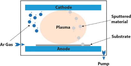
Simple diagram of a PVD system. Image Credit: KDF Technologies, LLC
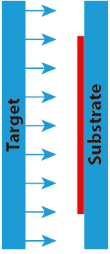
Side sputtering. Image Credit: KDF Technologies, LLC

Down sputtering. Image Credit: KDF Technologies, LLC
Thin Film Sputtering
Sputtering Modes
Thin film sputtering, including metal, dielectric, and reactive sputtering, can be performed using any of the following modes: DC sputtering, RF sputtering, Pulsed DC sputtering, and HIPIMS sputtering.
The earliest form of sputtering was DC (Direct Current), a straightforward and practical method primarily used for depositing metal films. As demand for thin film applications has grown, sputtering technology has continuously evolved to meet new industry challenges.
Today, several advanced sputtering configurations are available, including DC magnetron, RF (radio frequency), pulsed DC, and the more recent HIPIMS.
DC magnetron is an enhanced version of DC sputtering that significantly improves deposition rates. RF sputtering extends the technique to non-metallic materials, broadening its range of applications. Pulsed DC further refines DC magnetron sputtering, making it more effective for reactive processes. HIPIMS, the latest development, offers benefits such as harder coatings and improved step coverage in high-aspect-ratio features.

This information has been sourced, reviewed and adapted from materials provided by KDF Technologies, LLC.
For more information on this source, please visit KDF Technologies, LLC.