Sponsored by TescanReviewed by Ify IsiborNov 17 2026
TEM sample preparation has become more demanding for advanced semiconductor technology nodes due to complex device architectures and decreasing dimensions.
The need for TEM sample preparation is also expanding across automotive, display, and power semiconductor applications, which have historically used more mature technology nodes and larger feature sizes.
To address this industry trend, Tescan introduced the AI-powered TEM AutoPrep™ Pro software suite integrated with the SOLARIS 2 Ga FIB-SEM platform. This software enables reliable and unattended TEM sample preparation for 3 nm FinFET technology extracted from the Apple A17 Pro SoC fabricated by TSMC.
This AI-driven solution supports fully automated in-trench sample preparation, lift-out, and low-keV cleaning, achieving sample thicknesses below 100 nm.
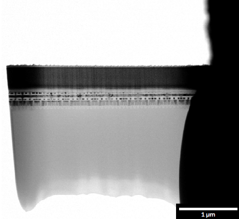
Fig 1. 3 nm FinFET technology, Fin-cut oriented lamella. Bright-field 100 keV STEM overview image. Image Credit: Tescan
A conventional TEM sample preparation process includes ROI localization, deposition of a Pt/C protective cap using either an electron beam or an ion beam, and coarse FIB milling at 30 kV with high beam current to create a lamella.
The lamella is then released and transferred to a TEM grid with a nanomanipulator, followed by thinning at low ion-beam currents (50–250 pA) to a thickness below 100 nm. A subsequent low-keV cleaning step is performed to reduce amorphization and ion implantation effects.
During the final thinning stage, manual SEM endpoint detection is used to maintain accurate feature targeting. This traditional workflow is labor-intensive, complex, and dependent on operator experience.

This information has been sourced, reviewed, and adapted from materials provided by Tescan.
For more information on this source, please visit Tescan.