| Perfection is not always ideal. In some cases, faults or defects may be exactly what is needed to make a particular material suitable for a particular application especially if those faults or defects can be tailored during processing of the material. Such is the case with certain high performance electronic materials. Normally, the ultimate in electronic properties is achieved with single crystal materials. Indeed, many of the materials used in today's electronic circuits and devices are monocrystalline. However, there are important exceptions, especially in cases for which compromises must be made between mechanical and electrical properties and costs. In these materials, grain boundaries play a vital role, affecting the electrical behaviour of the material and determining these compromises. In some cases, tailoring the structure of the grain boundaries has allowed researchers to design materials with ‘smart’ attributes that make them fit for purpose, stable and self-compensating. This article highlights new techniques for measuring the structure of grain boundaries in polycrystalline materials on a microscopic scale. These techniques will allow a deeper understanding of, and better modelling of macroscopic behaviour, such as the movement of electric current through polycrystalline materials, which is usually expressed in terms of ‘percolation theory’. Once this is better understood, materials and their grain boundary characteristics can be designed with improved electronic performance and, in some cases, smart capabilities to give more reliable electronic devices and systems with improved functionality and speed. High temperature superconductors on flexible substrates, thin film conductor tracks on silicon chips and thick film resistors on printed circuit boards and for surface mount technology are three examples of technologies that could benefit. Grain Boundaries and Current Flow Smart attributes have been designed into the grain boundaries of some conductor materials so that they are stable when conducting large currents. Electrical conductivity depends on both the density and the mobility of the charge carriers in a material. Figure 1a shows current flow through a homogeneous material. The value for the mobility of the charge carriers takes into account all inelastic scattering processes by which current flow is impeded. However, in a material containing grain boundaries, figure 1b, charge carriers may also be scattered at the interfaces between grains. So the movement of electric current is often far from the idealised picture of a swarm of electrons drifting through a homogeneous material under the influence of an applied electric field. | 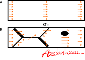
| | Figure 1. Conduction of current in (a) a homogeneous material and (b) a material containing grain boundaries and inclusions. | Exploiting Grain Boundaries By careful design of grain boundaries, this scattering can be put to good use. Obstructing or diverting the flow of electrons transfers momentum and energy to the source of the obstruction, causing localised heating. Other conducting pathways consequently become more highly stressed, as they have to carry more current. This can give rise to ‘thermal runaway’ effects in circuits, which are applied practically in devices known as high temperature superconducting fault current limiters. Runaway heating effects in these materials are used to limit the current in high power circuits, such as local power grids. These materials undergo a reversible transition from superconducting to ‘normal’ and so switch off any current overload. These smart devices could well replace the silicon power devices that are currently used for overload detection and control in power grids. Electronic Noise The movement of current through materials with significant grain boundary scattering is largely determined by the size of the angles between the grains. This often dictates the degree of scattering of the electrons. However, grain boundaries can affect a material’s behaviour in other ways. The electronic noise that accompanies fluctuations in the numbers of charge carriers is particularly important. Such fluctuations are caused by ‘generation-recombination’ mechanisms in which electron-hole pairs are produced or destroyed, which are often associated with grain boundaries. Texture Clearly, a material’s electronic behaviour can depend heavily on how well its texture is controlled. Such control requires accurate analysis. X-ray diffraction (XRD) techniques and electron diffraction in TEMs have traditionally been used to measure texture, but newer techniques based on computer analysis of electron backscattered patterns (EBSP) are gaining ground rapidly. SEM-based EBSP imaging techniques essentially bridge the gap between XRD and TEM-based diffraction analysis. The resolution obtained (less than one micron) is adequate for most purposes, and yet there is no need to make thin foils of the material, as with TEM. Texture analysis by x-ray pole figures and by the EBSP imaging techniques are complementary to some extent. X-ray techniques can sample a larger area (about 6x20mm) and a greater depth (10-5Oµm). They are relatively insensitive to surface defects and can quantify both weak and strong textures. EBSP imaging techniques look at smaller areas, are sensitive to surface defects and the beam size must be smaller than the grain size. However, they can differentiate between very strong textures that appear similar in x-ray pole figures and, most importantly, give information about grain misalignment and grain size by providing a detailed map of the crystallography of an area. In addition, a single analysis by EBSP allows simultaneous measurement of texture in all three axes, without the need to alter the orientation of the sample. Recent analysis using the complementary techniques of x-ray diffraction and electron backscattered imaging is helping to uncover the role of grain boundaries in determining the movement of percolative current in a material. This is accelerating the development of high temperature superconductor films on textured metallic substrates and next-generation conductor tracks on integrated circuits, and may even help tackle long-standing problems in thick film resistor materials. Each of these areas is addressed below. Superconductors The use of superconducting materials in electronic devices is desirable as they would improve performance and efficiency. High temperature superconductors are more stable than their low temperature counterparts and so are more able to cope with extreme magnetic fields, which is important if the materials are to be used in electrical machines and smart devices. As part of the drive to this goal, researchers in Europe are developing epitaxially-grown superconducting thin films on buffered nickel-based substrates, so called ‘coated superconductors’. Long Length Superconductors The aim is to produce long lengths of YBCO-coated conductor. This means that special attention must be paid to the grain boundary orientation of the metallic substrate being used and the buffer layers on which the superconducting coating is grown. Initial efforts to pass a high current through YBaCuO superconducting wires made by powder-in-tube and thick film techniques failed because grains in the material were not sufficiently aligned. This caused significant percolation of the current and consequently a dramatic reduction of the critical current density, Jc, as compared with a single crystal material, figure 2. | 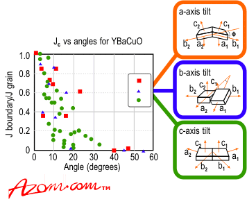
| | Figure 2. Variation of critical current density Jc with angle for three types of misalignment of YBaCuO grains. | Improving Performance Percolation of the current in YBCO layers is a problem even if the surface on which the material is epitaxially-grown is very smooth and the angle between the nickel-based substrate grains is minimised to 2-4 degrees. Researchers recognise the problem, and solving it will mean advanced analysis of the percolative effects in the coated conductors to improve the uniformity of the superconducting coating over, say, kilometre lengths. In all, three crucial aspects of coated superconductors need to be analysed by techniques such as EBSP, i.e. potential percolation of the current, cubicity of the metallic layers and smoothness of the metallic substrate surface. At the IRC in Superconductivity in Cambridge (UK), the need for nickel-alloy substrate development was recognised because pure nickel, annealed at elevated temperatures to induce cubic texture, is very soft and not easy to handle, especially at thicknesses below 50 microns. Nickel alloys can be made as thin as 13 microns thanks to their better mechanical properties. They should prove superior to pure nickel tapes, potentially providing much higher overall critical current density values for the final conductor. The packing density for coils wound with such tape in, say, magnets or transformers, will therefore be better. Integrated Circuits EBSP-based imaging and grain boundary control may also improve high current aluminium conducting tracks on silicon chips. Today’s chips carry huge numbers of devices, which are connected by narrow tracks of thin films of aluminium on the surface of the chip. With chip size shrinking and component density increasing, the electronics industry is constantly trying to minimise the space taken up by the conductor tracks. As a result, current density in the aluminium tracks has increased, causing problems with the phenomenon of electromigration, which causes the tracks to become degraded over a period of time. Electromigration Electromigration is the transport of material in an electrical conductor when a high current passes through it. It occurs in both pure materials and alloys. Electromigration is distinguished from the other diffusion phenomena such as concentration gradient diffusion, diffusion in a temperature gradient (thermomigration or chemical demixing) and stress-driven diffusion (creep or mechanodiffusion). The driving force for atomic migration comes from the interaction between the moving electrons and the stationary ions of the conductor material. In effect, the electrons push the ions in the direction of electron current flow through a succession of collisions. Aluminium or aluminium alloy (Al-4%Cu-1%Si) tracks usually carry current between semiconductor devices on the chip. These tracks are vulnerable to electromigration damage because they have to support high current densities of the order of 1011A.m-2. A 10mA current passes through an aluminium track typically 0.1 µm thick by 1µm wide. Operating temperature is typically 100°C, and under these conditions, grain boundary diffusion is the dominant transport mechanism. Flux Divergence Uniform electromigration is not as damaging as divergence in the flux. This can lead to material building up at, or being depleted from, certain points in the tracks, figure 3. The accumulation of material can produce hillocks (extrusions) or whiskers (long single crystals) and the corresponding depletion of material can leave voids. The hillocks and whiskers are usually much thicker than the rest of the film, and so can cause short circuits between adjacent tracks. Voids produce circuit failures by effectively severing tracks. These are all limiting factors in the further miniaturisation of integrated circuits. As track widths shrink, grain boundary effects become ever more important, and so materials with low angle grain boundaries are required to prevent electromigration problems arising. The solution is to produce highly textured aluminium tracks by in-groove melting and directional solidification, or by using copper-on-silicon technology being developed by IBM and others. | 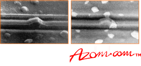
| | Figure 3. SEM micrographs of an aluminium electrical track showing non-uniform atom flow by precipitates blocking the track (left) and an EBSP image revealing the presence of the precipitate (right). | Improving Performance EBSP-based imaging techniques for mapping grain size distributions and delineating grain boundaries will be extremely useful tools for defining grain boundary misorientations. Analysis of conductor tracks on silicon using the OPAL EBSP imaging system shows the patterns centred around the 111 pole. The instrument highlights these areas and forms an ‘OPAL map’ of the material. This information will provide a better understanding of grain boundary electromigration in the integrated circuits of the future, not only for aluminium alloy tracks but also for the recently developed copper tracks pioneered by IBM. Some silicon chip plants, or ‘tabs’, are now equipped with on-line SEM inspection techniques for topographic analysis and compositional mapping, and the addition of EBSP for mapping texture could further enhance quality control. Thick Film Resistors Finally, EBSP analysis of grain boundary structures could help solve problems in the production of thick film resistors used in printed circuit boards. Screen-printed resistors based on ruthenium oxide have been used for many years in printed circuits and are an essential part of surface mount technology. These resistors must be extremely temperature stable, with near-zero temperature coefficient of resistance (TCR). The resistors must also have reproducible batch-to-batch resistivity over many decades of production, in order to maintain constant operating conditions for the devices and circuits on the chips. Composition of Inks The ‘inks’ used to make resistors consist of dispersions of ruthenium oxide powder and a binder such as borosilicate glass suspended in an organic materials, e.g. terpineol. The materials, the screen printing process parameters and the subsequent heat treatments have all been carefully researched so that resistor parameters, absolute value, TCR ‘tracking’, noise figures etc, can be obtained reproducibly. The result is a smart material system, in which fluctuations in processing parameters and in-service operating conditions (e.g. varying temperature) have been compensated for by successive enhancements to the material. This has been done largely empirically so far. Firing During a high temperature heat treatment, or ‘firing’, of the resistor material, the organic ‘carrier’ is burnt off to leave sintered ruthenium oxide particles embedded in a glassy matrix. This results in a conducting path through the material, where the ruthenium oxide grain boundaries are close to one another. However, the conduction mechanism is far from simple. In fact there are at least two conduction mechanisms. The first is the relatively straightforward conduction of electrons from one grain to an adjacent touching grain. The second mechanism can be described as ‘hopping’, in which electrons tunnel from one grain to another through the very thin insulating glassy layer. The predominant conduction mechanism depends on the relative amounts of glassy matrix and ruthenium oxide. Low resistivity resistors are made using a low volume fraction of glass, so that the degree of contact between the ruthenium oxide grains is relatively high. In high resistivity resistors on the other hand, the glass volume fraction is higher and the grains are kept further apart by the non-conducting glassy phase. Improving Performance To predict the movement of current through such materials is clearly a difficult job, and requires a sophisticated percolation model to deal with the range of resistivity values that can be produced. An additional complication is that the noise in these resistors depends on the generation-recombination mechanisms of charge carriers at the interfaces between grains. An understanding of the role of the grain boundaries is therefore doubly important for designing these systems. The use of the new EBSP imaging techniques for mapping the grain size distribution and grain boundary misorientation properties in fired resistors will shed further light on these complex materials. Such accurate analysis will lead to the production of better starting materials and improved processing of the next generation of reproducible and reliable printed resistors. In parallel, percolation current models will become increasingly accurate for a wide range of conducting materials. |