Jul 16 2008
Applied Materials, Inc. today announced its Applied Endura(R) Extensa(TM) PVD, the industry's only production-worthy system for depositing the critical barrier films for copper interconnects in sub-55nm memory chips. The Extensa system's unique titanium/titanium nitride (Ti/TiN) process technology enables diffusion barrier films with benchmark step coverage and less than 3% film thickness non-uniformity across the wafer, while achieving best-in-class defectivity and greater than 25% lower CoC than competing systems.
"The introduction of copper in memory devices presents unique film integration challenges due to the high voltages and dense packing requirements of memory cells," said Prabu Raja, vice president and general manager of Applied's Metal Deposition Products division. "Manufacturers are adopting new liner/barrier schemes as the most cost-effective way to get the performance benefits of copper. The Extensa system enables the robust integration of these critical new diffusion barriers with a proven, single-system solution that allows memory makers to realize high device yields down to the 32nm technology node and beyond."
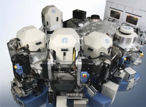
The Applied Extensa system's outstanding performance, already proven at multiple customer sites, is the result of several innovations in PVD technology that are implemented on the Extensa Ti/TiN deposition chamber. A novel dual-magnet PVD source with flux-shaping side electromagnets enables unmatched step coverage and defectivity below 10 particles at greater than or equal to 0.12 micrometer. The proprietary source technology also makes more efficient use of deposition material, delivering a 30% improvement in target life. In addition, the single piece chamber kit features Applied's proprietary CleanCoat(TM) technology for ease of maintenance and particle control.
Integrated on the highly successful Applied Endura platform, the Extensa technology offers Ti/TiN deposition solutions to support two key technology transitions in memory: the replacement of tantalum with Ti-based dielectric barriers in copper barrier/seed applications, and the introduction of copper-aluminum and copper-tungsten diffusion barriers that enable the most cost effective integration of copper with aluminum layers and tungsten vias.
Additional applications include contact liner for memory devices and, for logic customers, metal gate and silicide cap barrier deposition. The unique flexibility of the Endura architecture enables the industry's only integrated copper-aluminum barrier and aluminum fill solution on a single system.