Jul 16 2008
Applied Materials, Inc. today announced its Applied Producer® eHARP(TM) system, extending the production-proven HARP SACVD® gap-fill technology for critical STI device structures to 32nm and beyond. The eHARP process delivers void-free films to fill <30nm, >12:1 aspect ratio features - essential requirements for the fabrication of advanced memory and logic devices. Featuring proprietary new process innovations, the eHARP system's robust, high-density, strain-inducing films enable the scaling of conventional planar and emerging 3-D device structures.
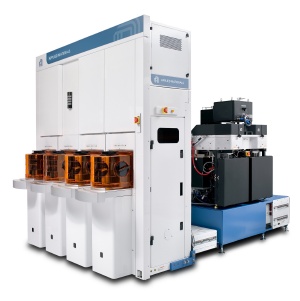 The Applied Producer eHARP system offers customers a gap-fill roadmap for critical shallow trench isolation structures for the 32nm and beyond technology nodes. (Photo: Business Wire)
“Applied has led the industry in providing the most advanced HDP-CVD(3) and SACVD gap-fill technologies over the last 14 years to meet customers’ most stringent process demands,” said Bill McClintock, vice president and general manager of Applied’s Dielectric Systems and CMP business unit. “With the Producer eHARP system, Applied offers customers an STI gap-fill roadmap beyond 32nm without significant changes to their process flow. Customers are very excited about the eHARP system’s capabilities, including major device manufacturers who have selected the eHARP system as tool of record for development and production in advanced logic and memory.”
The Producer eHARP technology offers the lowest overall cost-per-wafer compared to non-CVD gap-fill technologies. Virtually carbon-free, the eHARP film requires no protective liners or capping layers, easily integrates with conventional CMP processes and provides reliable, robust device isolation. In addition, the eHARP system’s proven process chemistries do not generate hazardous liquid byproducts that would necessitate specialized chemical disposal.
The eHARP process is available on Applied’s acclaimed Producer platform, which is used by virtually every chip manufacturer for advanced applications including etch, low k deposition, strain engineering, litho-enabling films, PECVD(4) and SACVD. More than 500 Producer systems have been shipped to customers for SACVD applications, any of which can be upgraded to run the eHARP process. For more information, visit http://appliedmaterials.com/products/eharp_4.html.
- SACVD = sub-atmospheric chemical vapor deposition
- STI = shallow trench isolation
- HDP-CVD = high density plasma CVD
- PECVD = plasma enhanced CVD