May 27 2009
Novellus Systems, Inc. (NASDAQ: NVLS) is a leading provider of advanced process equipment for the global semiconductor industry, has developed the IONX XL (eXtended Life) Ta(N) barrier process for the 3x/2xnm memory node, based on Novellus' PVD Hollow Cathode Magnetron (HCM) deposition technology.
Ten years after the introduction of copper metallization for logic device manufacturing, Physical Vapor Deposition (PVD) copper barrier-seed and copper electrochemical deposition (ECD) are now being used for the production of DRAM and Flash memory chips. The memory transition from aluminum metallization to copper interconnects is being driven by the technological challenges associated with device scaling and the need to reduce memory chip manufacturing cost.
One of the key components of a copper memory interconnect is the PVD tantalum nitride (Ta(N)) barrier layer that provides the necessary copper diffusion resistance, as well as wettability for the subsequent copper seed layer. For memory manufacturers, the challenge comes with depositing this barrier film in advanced device structures that can possess up to 30 percent smaller critical dimensions (CD) than those found in logic applications. For these aggressive geometries, planar PVD is limited by shadowing effects that can cause incomplete film coverage due to overhang at the top corner of the trench or via, in turn leading to inadequate copper fill and yield loss. Some planar PVD barrier solutions are investigating the incorporation of more expensive CVD layers to mitigate these effects. Compounding these challenges is the fact that Ta(N) barriers also need to be very thin (less than 120 Angstrom in the field) in order to minimize the volume fraction of high resistivity Ta(N) relative to low resistivity copper within the feature.
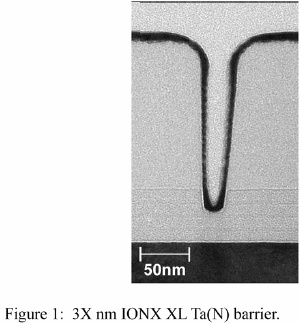
This PVD-only barrier process deposits high quality films with excellent step coverage for high aspect ratio memory structures. The conformal Ta(N) films deposited with this technology are the result of an increased plasma density and more effective control of the ionized flux that reaches the wafer surface. The figure shows a thin, highly conformal IONX XL Ta(N) barrier layer deposited into a 3xnm memory device trench with no top corner overhang. Not only does this robust copper barrier process meet the technical challenges of advanced memory, but it also results in a 40 percent reduction in the tantalum Cost of Consumables (CoC) compared to competitive market offerings. A 100,000 wafer-starts-per-month memory megafab using two levels of metal can save approximately $1M a year in consumable costs through more efficient utilization of the tantalum target material.
"As memory technology transitions to copper interconnects, the 3x/2xnm device dimensions are placing stringent technical and cost requirements on the Ta(N) barrier layer," said Dr. Wai-Fan Yau, general manager for Novellus' Integrated Metals Business Unit. "The new IONX XL barrier film meets these advanced technical demands and also provides a significant reduction in consumable costs."