An international team led by a chemistry professor at Penn State University (PSU), John Badding, has developed crystalline materials that enable integration of high-speed electronic components to an optical fiber.
 For the first time, researchers have developed crystalline materials that allow an optical fiber to have integrated, high-speed electronic functions.
The integrated optical fibers have several potential applications, including highly accurate remote-sensing devices, enhanced laser technology, telecommunications and various other hybrid electronic and optical technologies.
Currently, one of the major technological challenges in the market is to exchange information between electronic and optical systems in a fast and efficient manner. The existing technologies have merged optical fibers with chips in unproductive ways. The chips or silicon-based integrated circuits play a major role in most semiconductor devices like cell phones, computers, LEDs and solar cells. But, it is difficult to merge optical fibers and electronic chips. One of the reasons is that the optical fibers are round in shape, whereas chips are flat. Hence, just shaping the link between the fibers and chips becomes a major challenge. In addition, arrangement of pieces that are too small is another important challenge. The PSU team has worked on a different method to meet these challenges.
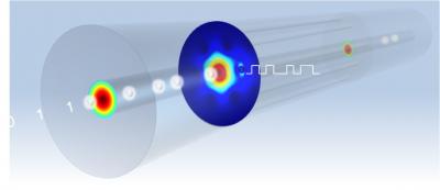
Researchers have identified a way to develop a new type of optical fiber with integrated electronic components, rather than merging a round optical fiber with a flat electronic chip. With the use of high-pressure chemistry methods, they deposited semiconducting materials directly into small holes of optical fibers. Thus, they fabricated the semiconductor junction, where the entire electronic action occurs, exactly into the optical fiber. The current work opens up new opportunities for optoelectronic applications. It also has potential applications in non-telecommunications. One of the team member and a researcher at the University of Southampton, Pier J. A. Sazio remarked that their process can cost less as it requires simple equipment, whereas conventional chip fabrication needs multimillion-dollar facilities. He also added that one of the major objectives of this research is to develop a faster, cheaper, and highly efficient all-fiber network.