Apr 8 2015
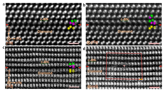 Figure: (a and b) HAADF STEM images of c-BN/diamond interface viewed in direction parallel to [1-10] zone axis, (a) coherent area without defects, (b) area with defects, (c and d) HAADF STEM images of c-BN/diamond interface viewed in direction parallel to [11-2] zone axis, (c) area without defects, and (d) area with defects. Partial dislocations are observable. By comparing (c) and (d), a Burgers vector, which characterizes partial dislocations, of 1/4<1-10> was determined. All scale bars are 0.5 nm in length.
A research team from the Tohoku University and Advanced Institute for Materials Research in association with Group Leader Takashi Taniguchi at the National Institute for Materials Science and Japan Fine Ceramics Center (JFCC) has identified, for the first time, the atomic structure and bonding mechanism of coherent interfaces between the hardest and second hardest materials, diamond and cubic boron nitride.
The team led by Associate Professor Zhongchang Wang, Professor Yuichi Ikuhara and Assistant Professor Chunlin Chen at the Advanced Institute for Materials Research used the first-principles calculation and a sophisticated super-high-resolution scanning transmission electron microscope to identify the bonding mechanism.
The researchers tried to generate new functional materials by observing lattice defects in crystals such as grain boundaries and interfaces, dislocation, studying their atomic structures and monitoring lattice defects.
Using the elaborate first principles-based theoretical calculation and the simultaneous use of atomic-resolution scanning transmission electron microscopy that has achieved several technological breakthroughs in recent years, the researchers were able to identify the bonding of carbon and boron in coherent interfaces between cubic boron nitride and diamond. Dislocations, a kind of crystal defect, features a characteristic structure.
The findings could help in the future development of new devices with materials having modified properties. The improved properties may result from monitoring these kind of defect structures, research and development of new functional materials, and design of new devices comprising lattice defect structures.
The research paper titled “Misfit accommodation mechanism at the heterointerface between diamond and cubic boron nitride” was published in the Nature Communications journal on February 17, 2015.