Dec 4 2017
A team of scientists at KIT have obtained three-dimensional insights into the interior of crystals by employing non-destructive imaging methods. They have established the vital data about line-shaped defects that immensely influence the deformation behavior of crystals.
These dislocations hinder the creation of computer chips. Based on a report in the Physical Review Letters, the scientists merge two X-ray methods with an exceptional type of light microscopy.
 When processing semiconductor wafers, small surface defects may lead to large defects inside and to steps on large surface areas. (Figure: D. Hänschke/KIT)
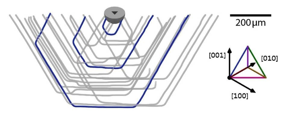
It is possible for even a few dislocations in silicon wafers to result in defective computer chips, thus, leading to undesired production rejects. “It is therefore important to understand how a minor mechanical surface defect propagates into the depth of the crystal under typical process impacts, such as heat,” says Dr. Daniel Hänschke, physicist of KIT’s Institute for Photon Science and Synchrotron Radiation. His team has succeeded in accurately measuring dislocations and then analyzing their interactions with each other and also with external impacts. The scientists studied how just one surface defect spreads into an armada of hexagonal defect lines, while fully undamaged areas could continue to be in the center of this type of a three-dimensional network. “The resulting collective movement can raise or lower large surface areas on the opposite side of the wafer and cause the formation of steps, which may adversely affect the fabrication and function of microstructures,” Hänschke points out.
Incorporated with mathematical model calculations, the results enable enhancing the understanding of the fundamental physical principles.
Models used so far are mainly based on data measured by electron microscopy in very small crystal samples, our method can also be applied to study large, flat crystals, such as commercially available wafers, this is the only way to determine detailed relationships between the initial, minute original damage and the resulting extensive crystal deformations that may cause major problems far away from the onset of the defect.
Dr. Elias Hamann, another member of the team at KIT
The new measurement method incorporates X-ray techniques at the ESRF European synchrotron in Grenoble and the KARA synchrotron of KIT with CDIC light microscopy. The results will help enhance the currently available models for the prognosis of defect propagation and defect formation, thus offering indications of how to optimize the fabrication process of computer chips. The number of transistors positioned on a square centimeter of a wafer surface is known to have already reached several billions, with growing tendency. Even tiny defects in and on the crystal may cause thousands of these tiny circuits to fail and the equivalent chips to be ineffectual. Industry is immensely interested in additionally reducing the defect rate in the future.