Apr 25 2018
The future generation of solid-state lighting, high-frequency communication systems, and energy-efficient power electronics is dependent on materials called wide-bandgap semiconductors.
In contrast to silicon-based circuits, circuits formed with these materials have the ability to function with lower power losses and at considerably higher power densities. These materials have been at the center of a revolution in LED lighting, which resulted in the Nobel Prize in physics for the year 2014.
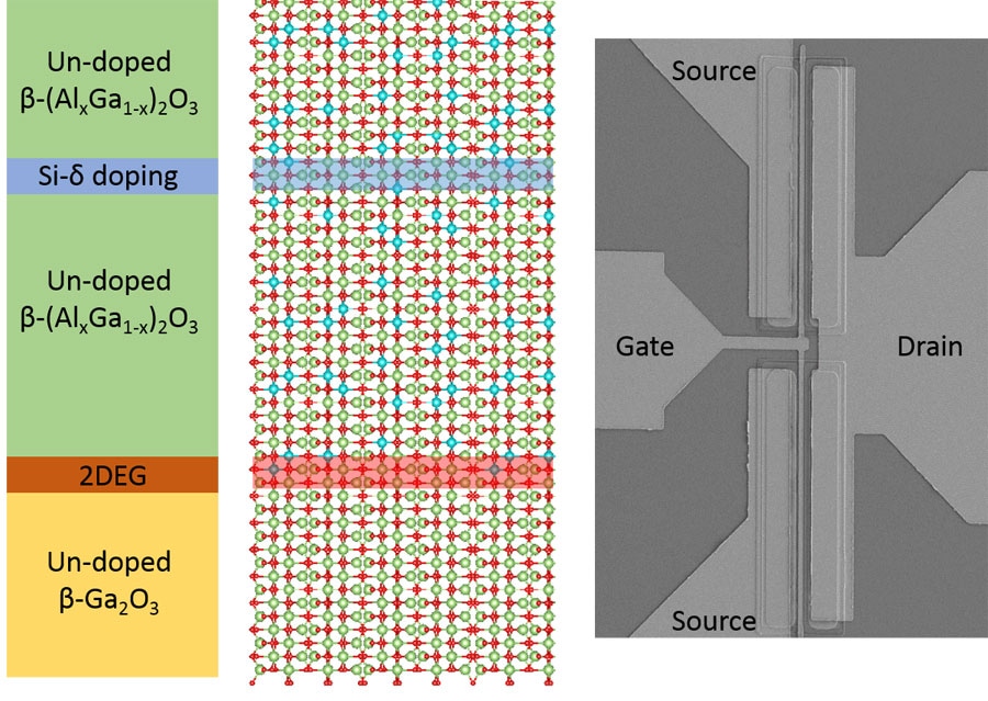 Schematic stack and the scanning electron microscopic image of the β-(AlxGa1−x)2O3/Ga2O3 modulation-doped field effect transistor. (Image credit: Choong Hee Lee and Yuewei Zhang)
After conducting innovative experiments, which have been published in Applied Physics Letters from AIP Publishing, scientists have demonstrated that gallium oxide (Ga2O3), a wide-bandgap semiconductor, can be engineered into nanometer-scale structures that enable considerably rapid movement of electrons within the crystal structure. Since electrons in Ga2O3 can move with much ease, it could turn out to be a promising material for applications such as energy-efficient power electronics and high-frequency communication systems.
“Gallium oxide has the potential to enable transistors that would surpass current technology,” stated Siddharth Rajan of Ohio State University, who headed the study.
Since the bandgap (or the energy requite to excite an electron to make it conductive) of Ga2O3 is one of the largest among those of the wide bandgap materials being developed as substitutes for silicon, it is specifically useful for high-frequency and high-power devices. It is also distinctive among wide bandgap semiconductors because it can be directly produced from its molten form, thereby facilitating large-scale production of high-quality crystals.
For the material to be used in electronic devices, the electrons in it should be in a position to easily move under an electric field, a property known as high electron mobility. “That’s a key parameter for any device,” stated Rajan. In general, for a semiconductor to be populated with electrons, the material is doped with other elements. However, the difficulty is that the electrons are also scattered by dopants, thereby restricting the mobility of electrons in the material.
To overcome this difficulty, the scientists adopted a method called modulation doping. This strategy was initially developed by Takashi Mimura in 1979 to develop a gallium arsenide high-electron mobility transistor, which was awarded the 2017 Kyoto Prize. Although this method is commonly used at present to enable high electron mobility, its application to Ga2O3 is a relatively new strategy.
In their study, the scientists developed a so-called semiconductor heterostructure, forming an atomically perfect interface between Ga2O3 and its alloy with aluminum gallium oxide and aluminum—two semiconductors that have different energy gaps in spite of their same crystal structure. A sheet of electron-contributing impurities with a thickness of just few atoms is embedded within the aluminum gallium oxide, a few nanometers away from the interface. The contributed electrons are transferred into the Ga2O3, thus forming a 2D electron gas. However, since the electrons are now also isolated from the dopants (hence the term modulation doping) by a few nanometers within the aluminum gallium oxide, they remain highly mobile and get scattered considerably less.
The scientists achieved record electron mobilities with the help of this method. They could also observe Shubnikov-de Haas oscillations, a quantum phenomenon in which the resistance of the material starts oscillating when the strength of an external magnetic field is increased. These oscillations validate the formation of the high-mobility 2D electron gas and enable the scientists to measure vital material properties.
Rajan remarked that these modulation-doped structures could result in the formation of a new category of quantum structures and electronics that exploits the potential of Ga2O3.