Dec 31 2018
Headed by Professor Tetsuo Endoh at Tohoku University, a research team has successfully created a 128 Mb-density spin-transfer torque magnetoresistive random access memory (STT-MRAM) with the world’s fastest write speed of 14 ns for use in embedded memory applications, like the cache in AI and IOT.
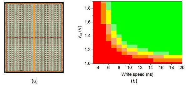 (a) Mock-up image of 128 Mb-density STT-MRAM. (b) Shmoo plot for write speed versus supply voltage, which shows the measured operation bit rate at each speed and voltage in color gradation. (Image credit: Tohoku University)
With the world’s fastest write speed for use in embedded memory applications and with a density of more than 100 Mb, the STT-MRAM will present new opportunities to produce large-capacity STT-MRAM on a massive scale.
STT-MRAM can operate at high speed and consumes only minimum power because it is designed to retain data even when the power is off. Thanks to these features, STT-MRAM is attracting a great deal of attention as the state-of-the-art technology for a number of applications like main memory, embedded memory, and logic. Risk mass-production will be started in 2018, according to three large semiconductor fabrication plants.
Since memory is a critical part of handheld devices, computer systems, and storage, its reliability and performance are extremely important for green energy solutions.
The present capacity range of the STT-MRAM is 8–40 Mb. However, STT-MRAM can be made more practical by increasing the memory density. At the Center for Innovative Integrated Electronic Systems (CIES), the team has boosted the STT-MRAM’s memory density by thoroughly creating STT-MRAMs in which magnetic tunnel junctions, or MTJs, are incorporated with CMOS. This will considerably lower the power consumption of embedded memory like eFlash memory and cache.
A range of process developments is made to miniaturize MTJs. In order to reduce the memory size required for higher density STT-MRAM, the MTJs were directly formed on via holes—tiny openings that enable a conductive connection between the varied layers of a semiconductor device. With the help of the reduced size memory cell, the research team has successfully developed a 128 Mb-density STT-MRAM and also constructed a chip.
The team determined a write speed of subarray within the fabricated chip. Consequently, high-speed operation with 14 ns was shown at a low power supply voltage of just 1.2 V. So far, this is the world’s fastest write speed operation in an STT-MRAM chip with a density of more than 100 Mb.
The study results were presented at the 2018 International Electron Devices Meeting held on December 5th, 2018, in San Francisco, United States.
The STT-MRAM R&D program, an industry-academic collaboration of JST-ACCEL and the CIES consortium, supported the study.