Mar 18 2019
A new fabrication process for the multilayer processing of silk-based microelectronics has been designed by the researchers at KAIST. This technology for developing a biodegradable silk fibroin film permits microfabrication with metal or polymer structures produced from photolithography.
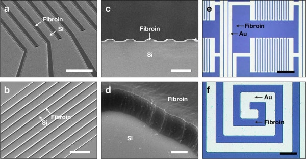 Fibroin microstructures and metal patterns on a fibroin produced by using the AMoS mask. (Image credit: KAIST)
This method, which involves using silk fibroin patterns, can play an important role in the application of silk fibroin-based biodegradable electronic devices or localized drug delivery.
Silk fibroins are very good candidates for the implantable biomedical devices owing to their properties such as biodegradability, biocompatibility, flexibility, and transparency. Also, they have been used as functional microstructures and biodegradable films in biomedical applications. Yet, strong etching solutions and solvents are needed for the traditional microfabrication processes to alter the structure of silk fibroins.
Professor Hyunjoo J. Lee from the School of Electrical Engineering and her colleagues have devised a new process, called aluminum hard mask on silk fibroin (AMoS), to keep the silk fibroin from being impaired during the process. AMoS has the potential to micropattern various layers of fibroin and inorganic materials, like metal and dielectrics, with high-precision microscale alignment. This process is also capable of creating silk fibroin patterns on devices or patterns on the silk fibroin thin films with other materials using photolithography, a basic technology of the existing microfabrication process.
The researchers have been successful in culturing primary neurons on the processed silk fibroin micropatterns and asserted that silk fibroin had excellent biocompatibility in the pre- and post-fabrication process and can be used in the implanted biological devices.
Using this technology, the research team developed the multilayer micropatterning of fibroin films on a silk fibroin substrate and created a biodegradable microelectric circuit with resistors and silk fibroin dielectric capacitors in a silicon wafer with wide areas.
The team also placed the micropattern of the silk fibroin thin film adjacent to the flexible polymer-based brain electrode using this technology and asserted that the dye molecules arranged on the silk fibroin were shifted successfully from the micropatterns.
This technology facilitates wafer-scale, large-area processing of sensitive materials. We expect it to be applied to a wide range of biomedical devices in the future. Using the silk fibroin with micro-patterned brain electrodes can open up many new possibilities in research on brain circuits by mounting drugs that restrict or promote brain cell activities.
Hyunjoo J. Lee, Professor, School of Electrical Engineering, KAIST
This study, which was performed in collaboration with Dr Nakwon Choi from KAIST and led by PhD candidate Geon Kook, has been published in ACS AMI on January 16th, 2019.