An organic solar cell is considered a promising seed of innovation in the renewable energy industry as it is a flexible, lightweight, cost-efficient, and green device.
 (a) Hopping conduction in disordered junction, (b) band conduction in crystalline junction. (Image credit: NINS/IMS)
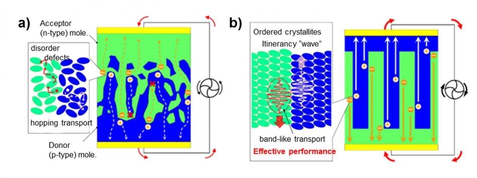
However, the energy conversion efficiency of the organic solar cell is less when compared to those of conventional silicon solar cells.
In semiconductor solar cells, the light is turned into an energized pair of a hole (positive carrier) and an electron (negative carrier) at the “pn junction” interface at two semiconductor layers in the cell. In each layer of the semiconductors, acceptor (electron catching; n-type) and donor (electron pitching; p-type) molecules face each other as the perfect pn junction.
Increasing the number of such solar “batteries” in the cell needs large area of the pn junction, so that a complex “bulkhetero” pn junction—which is a folded interface similar to pleats— has been created. In such a complex structure like a maze, it is not easy for the created carriers to reach output electrodes of the cell, since the molecules are arranged unevenly; simply put, the crystallinity is low.
The carrier—an electron or a hole—must delocalize between molecules as a matter wave in order to efficiently achieve a high transport. The wave nature of the carriers is revealed by the ordered arrangement of molecules.
Scientists at the Institute for Molecular Science (IMS), Japan Synchrotron Radiation Research Institute (JASRI) and Tokyo University of Science have successfully developed the organic semiconductor pn junction with high crystallinity. In the production process of the junction, the acceptor (perfluoropentacene) molecules were layered on to the single crystal of the donor molecules (pentacene) in a well-organized manner through the molecular beam epitaxy (MBE) method.
Using the angle-resolved photoelectron spectroscopy, the electronic structures of the crystalline pn junction were observed and it was demonstrated that the layer of the acceptor molecules creates the valence band, which is a proof of bringing up the wave nature. The outcome of the current research demonstrates that the MBE enables the fabrication of the crystalline pn junction, which may invoke the wave nature of the holes as well as the electrons.
It is possible to adjust the functions of organic semiconductors by designing the structures of basic organic molecules. The production technology of the crystalline pn junctions using various organic molecules allows the new model organic solar cells to be achieved with high energy conversion efficiency.