Image Credit: University of Glasgow.
Engineers from the Bendable Electronics and Sensing Technologies (BEST) group at the University of Glasgow have explained how they organized and enhanced the traditional process for developing flexible large-area electronics. The study has been published in the journal npj Flexible Electronics.
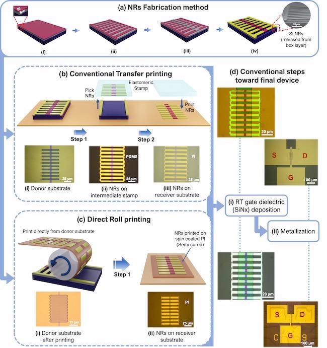
So far, highly sophisticated flexible electronics have been primarily manufactured using a process known as transfer printing. It is a three-level stamping process, similar to receiving an ink stamp in a passport during a foreign visit.
Initially, a silicon-based semiconductor nanostructure is engineered and built on a surface called a substrate. Next, the nanostructure is taken from the substrate using a soft polymeric stamp. Finally, the nanostructure is shifted from the stamp to a different flexible substrate, ready for use in bendable devices like health monitors, bendable displays, and soft robotics.
But the transfer printing process includes several limitations, making it hard to manufacture more large-scale and complicated flexible devices. Gaining accurate control of crucial variables such as the speed of transfer, as well as the adhesion and orientation of the nanostructure, has made it hard to ensure identical stamps every time.
A badly stamped passport can cause difficulty to the traveler in reading it; similarly, a misaligned or incomplete polymetric stamp onto the last substrate can deliver a low-standard electronic performance or even lead to device malfunction.
Although processes were developed to deliver effective stamping transfer, they mainly need extra equipment like magnets and lasers, which causes an increase in manufacturing charges.
The Glasgow team had adopted a different method, eliminating the second stage of the traditional printing process. This process prints silicon directly onto a flexible surface instead of transferring nanostructures to a soft polymeric stamp before being shifted to the final substrate. This new process is known as “direct roll transfer.”
The process starts with the fabrication of a thin silicon nanostructure, measuring less than 100 nm. The receiving substrate, a flexible and high-performance plastic foil material known as polyimide, is then covered using an ultrathin layer of chemicals to enhance adhesion.
The substrate prepared is then wrapped around a metal tube, and a computer-controlled machine designed by the team rolls the tube over the silicon wafer. This makes it a flexible material.
After keenly regulating the process, the team created highly uniform prints over an area measuring around 10 cm2, along with a 95% transfer yield. This value is remarkably higher than many of the traditional transfer printing processes available at the nanometer scale.
Although we used a square silicon wafer sample of 3 cm on each side in the process we discuss in this paper, the size of the flexible donor substrate is the only limit on the size of silicon wafers we can print. It’s very likely that we can scale up the process and create very complex high-performance flexible electronics, which opens the door to many potential applications.
Ravinder Dahiya, Professor and Leader of BEST Group, James Watt School of Engineering, University of Glasgow
Dahiya continued, “The performance we’ve seen from the transistors we’ve printed onto flexible surfaces in the lab has been similar to the performance of comparable CMOS devices—the workhorse chips which control many everyday electronics.”
“That means that this type of flexible electronics could be sophisticated enough to integrate flexible controllers into LED arrays, for example, potentially allowing the creation of self-contained digital displays which could be rolled up when not in use. Layers of a flexible material stretched over prosthetic limbs could provide amputees with better control over their prosthetics, or even integrate sensors to give users a sense of ‘touch’, added Dahiya.
It’s a simpler process capable of producing high-performance flexible electronics with results as good as, if not better, than conventional silicon-based electronics. It’s also potentially cheaper and more resource-efficient, because it uses less material, and better for the environment, because it produces less waste in the form of unusable transfers.
Ravinder Dahiya, Professor and Leader of BEST Group, James Watt School of Engineering, University of Glasgow
This study was financially supported by the Engineering and Physical Sciences Research Council (EPSRC).
Direct Roll Printing of High-Performance Electronics
Video Credit: University of Glasgow.
Journal Reference:
Zumeit, A., et al. (2021) Direct roll transfer printed silicon nanoribbon arrays based high-performance flexible electronics. npj Flexible Electronics. doi.org/10.1038/s41528-021-00116-w.