A team of researchers from Taiwan conducted an extensive review, published in the journal Advanced Science, on various optical inspection techniques available to characterize a variety of 2D materials including graphene, transition metal dichalcogenides (TMDCs), hexagonal boron nitride (h-BN), group-III monochalcogenides, black phosphorus (BP), and group-IV monochalcogenides.
The research team led by Professor Hsuen-Li Chen of the Materials Science and Engineering Department, National Taiwan University, also identified some of the challenges and opportunities faced when optically inspecting 2D materials, such as mechanical exfoliation and wafer-scale growth.
Due to the unique chemical and physical properties of 2D materials, including layered structure, high-surface-area, layer-dependent optical bandgap, and variation of chemical composition they are considered to be key to the development of numerous applications in areas such as biomedicine, thermoelectric, sensing, and energy storage.
Optical Inspection
Atomically thin 2D materials can be used for advancing the next generation of devices such as photodetectors, optical modulators and switches, light-emitting devices, transistors, and sensors. Therefore, the basic structural and physical make-up of these materials are key for their overall performance in these devices.
Thus, having a good technique for the characterization of the properties of 2D materials at the atomic level is deemed a necessary and vital tool. Among the various existing methods for evaluating the properties of 2D materials, optical inspection can be a powerful tool:
When the probe light is applied incident to the analytical material (in this case, a 2D material), interactions between the light and the atoms or electrons can reveal much information about the fine structural characteristics
Professor Hsuen-Li Chen, Professor, Materials Science and Engineering Department, National Taiwan University
In their comprehensive study, Prof. Chen and his team assessed the available methods for optical inspection of 2D materials including common optical spectroscopy, Raman spectroscopy, Fourier Transform Infrared (FTIR) spectroscopy, and x-ray scattering amongst others. Prof. Chen states that he and his team wanted to address, “the current status—and the challenges and future trends—of the methods available for optical inspection of the characteristics of 2D materials.”
Optical inspection not only allows researchers to determine the properties of a given material such as graphene but also facilitates the further development of their application. For example, using optical inspection methods it has been both theoretically and experimentally demonstrated that the Fermi level in graphene, the first 2D material discovered, can be tuned meaning its optical and electrical properties can in effect be controlled.
Mechanical Exfoliation Vs Wafer Scale Growth
In addition to graphene, TMDCs have been subjected to intense and widespread analysis throughout various research fields. It has been determined that TMDCs possess a number of properties complementary to those of graphene making them good candidates for high-speed electronic and optoelectronic devices.
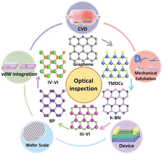
Schematic representation of the most widely studied 2D materials, including graphene, transition metal dichalcogenides (TMDCs), hexagonal boron nitride (h-BN), group-III monochalcogenides (III-VI), black phosphorus (BP), and group-IV monochalcogenides (IV-VI), and the developmental progress of 2D materials from mechanical exfoliation to the implementation of 2D material-based devices. Image Credit: Lee, Y.-C et al., Advanced Science
In the early stages of 2D material research, around the mid-2000s, mechanical exfoliation was the most popular method of ‘top-down’ preparation of monolayers. Applying the ‘Scotch tape' method, it was possible to assess the basic properties of graphene, however, this method is not ideal for upscaling production of 2D materials and does not always facilitate good control over the structural and physical properties of the layers.
Furthermore, using mechanical exfoliation makes locating ultrathin 2D materials on substrates a challenging experience. However, Chen and his team identified an optical microscopy (OM) method that allows for rapid location of monolayer or few-layer 2D materials when they are prepared on substrates demonstrating enhanced visibility.
To overcome some of the challenges associated with mechanical exfoliation researchers have developed a method of growing wafer-scale single-crystal h-BN films on molten gold surfaces. This indicates the possibility to also grow other 2D materials on the wafer scale.
Prof Chen states, “To facilitate the development of wafer-scale growth techniques for various 2D materials, in situ monitoring of the global properties of the synthesized 2D materials, especially their structural quality, would be critical when adjusting the growth parameters.”
Further developing wafer-scale growth methods may also open the window of opportunity for upscaling methods and boost the practical application potential in various devices. Optical inspection techniques also allow materials to be characterized non-destructively making them good for in-situ global inspection of 2D material properties.
Future Development
The Taiwan-based team identified that in particular Raman and PL spectroscopies are powerful tools for characterizing 2D materials, Optical spectroscopy and spectroscopic ellipsometry are alternative methods for evaluating 2D materials on the wafer-scale, because of their relatively larger spot sizes.
Chen and his team hope that their detailed evaluation and review of various optical inspection techniques will lead to significant progress in the development of novel 2D material-based devices.
Chen states, “This comprehensive review of the current status and perspective of future trends for optical inspection of the structural properties of 2D materials will facilitate the development of next-generation 2D material-based devices.”
References:
Lee, Y.-C., Chang, S.-W., Chen, S.-H., Chen, S.-L., Chen, H.-L., Optical Inspection of 2D Materials: From Mechanical Exfoliation to Wafer-Scale Growth and Beyond. Adv. Sci. 2021, 2102128. https://onlinelibrary.wiley.com/doi/full/10.1002/advs.202102128
Disclaimer: The views expressed here are those of the author expressed in their private capacity and do not necessarily represent the views of AZoM.com Limited T/A AZoNetwork the owner and operator of this website. This disclaimer forms part of the Terms and conditions of use of this website.