Heteroepitaxial approaches to crystal growth and material deposition remain one of the most popular and widely used approaches to forming crystalline layers on substrates.
Heteroepitaxial layers typically offer well-defined orientations, and these methods represent an ideal means of growing and integrating crystalline films of materials where it is not otherwise possible to obtain crystals.
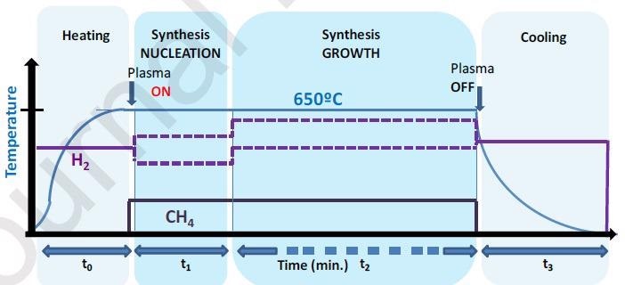
Two-step synthesis. Temperature and partial pressures profile with H2 diluent (in purple, dashed line). Temperature: 650 ºC (nucleation & growth), t0=40 min, t1=4 min, t2=120 min, t3=40 min. H2 flow is modified between 20-50 sccm. CH4 flow=2 sccm. Plasma power: 200W. Image Credit: R. Muñoz et al., Applied Surface Science
There are notable limits to conventional heteroepitaxial growth, and this process is only compatible with materials exhibiting coincident lattice constants. This ensures performance-impairing interfacial defects or dislocations are kept to a minimum.
Certain 2D heterostructures can be created by directly stacking mechanically exfoliated flakes of appropriate materials.
These 2D materials have facilitated the development of an array of photonic and electronic devices, with mechanically exfoliated monolayer and multilayer graphene sheets found to offer excellent potential for use as high-performance electrodes in heterostructured devices.
Mechanically exfoliated graphene-MoS2 heterostructures’ efficient charge transfer has also led to never-before-seen levels of responsivity and sensitivity when used in room-temperature photodetection applications.
These applications all offer excellent promise in terms of their performance, applicability, and versatility, but their widespread uptake and scalability have thus far been hindered by mechanical exfoliation methods’ low production yield, time-consuming production processes, and the chance of contaminated transferred crystals.
In order to mitigate these risks and address these barriers to industrialization, it is of paramount importance to develop a truly scalable approach to fabrication.
With this in mind, advanced techniques involving direct heterostructure growth via MoS2/graphene and graphene/MoS2 are already being developed, with a recent paper in the Applied Surface Science journal presenting a novel approach to directly synthesizing graphene films on MoS2.
This is performed at low temperatures via plasma-assisted chemical vapor deposition (CVD) using CH4 and H2 as precursors. The researchers' highlight that there have been limited attempts to directly grow graphene on MoS2 due to the need for complex, multi-step protocols that frequently lead to amorphous carbon deposition.
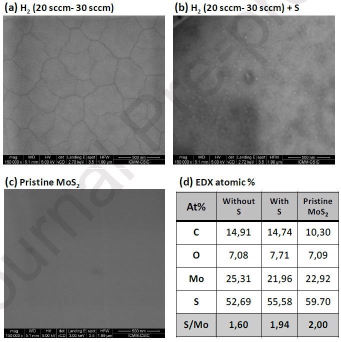
SEM images of the graphene films grown without S (a), with S (b) and pristine MoS2 topography (c). (d) EDX % atomic semiquantitative analysis of the previous samples. We include the C, O, Mo, S in the quantitative analysis and normalize the S/Mo ratio = 2 with the values obtained in the pristine MoS2 single crystal as a standard. Image Credit: R. Muñoz et al., Applied Surface Science
Instead, this new CVD-based approach enables the direct synthesis of graphene films on an exfoliated MoS2 single-crystal surface by leveraging a comparatively straightforward two-step synthesis protocol to manage the nucleation and growth stages of the film via distinct processes.
By monitoring and adjusting specific parameters including temperature, processing time, partial pressures, and precursor gas flow, the researchers were successful in both increasing the grain size of graphene and enhancing the quality of the MoS2 interface.
The researchers also introduced external S species to the vapor in order to effectively heal natural or induced S vacancies in the MoS2 substrate, helping to ensure a more uniform surface.
A series of characterization experiments were performed to evaluate the healing effect of S on the MoS2 structure, with surface chemical analysis via XPS and cross-section HR-TEM morphology confidently confirming that the defects or vacancies in the MoS2 substrate are notably lessened through the use of S vapor during synthesis.
Conductive-AFM was used to perform a series of graphene conductance measurements, highlighting the impact of MoS2’s final stoichiometry on its conductance.
Perhaps the most notable advantage of this low-temperature growth is that it is highly scalable. It also enables the creation of a clean, chemically controlled graphene-semiconductor interface which could see a plethora of uses when integrated into heterostructures destined for use in advanced electronic and photonic devices.
Because it is possible to customize the grown graphene films’ structure and its chemistry at its interface with MoS2, there is considerable scope to further modify these synthesis parameters for increasing optimization and customization according to specific application needs.
Plasma-assisted CVD is an intrinsically scalable method that offers a number of advantages, not least due to its comparatively straightforward and efficient implementation versus its mechanical exfoliation counterpart.
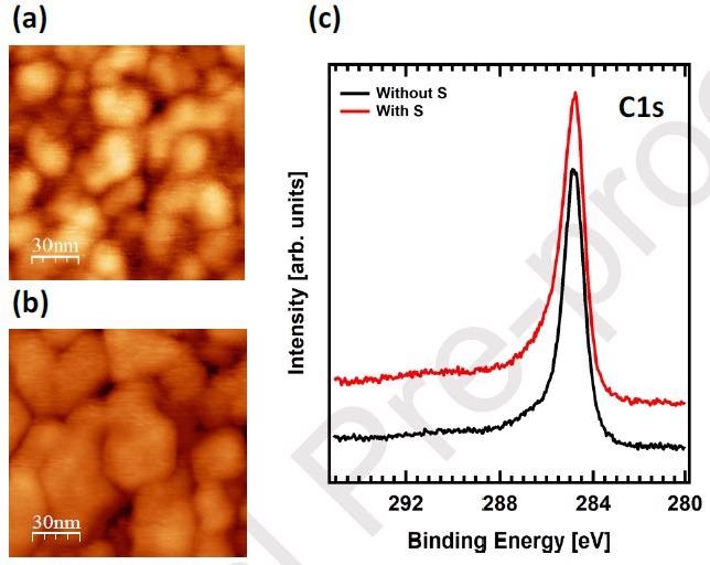
(a, b) High resolution AFM topographic image of the samples deposited with H2 flow (20 sccm- 30 sccm) without (a) and with S (b). (c) XPS C 1s core level spectra of the samples deposited in two steps with H2 flow (20 sccm-30 sccm) without S (black line) and with S (red line). Image Credit: R. Muñoz et al., Applied Surface Science
The advantages and potential uses of graphene are well documented, particularly its application in the semiconductor field where it has been mooted as a possible successor to silicon throughout the industry.
These processes could also be applied to other semiconducting van der Waals heterostructures, potentially expanding their use cases into a range of sectors and industries.
Disclaimer: The views expressed here are those of the author expressed in their private capacity and do not necessarily represent the views of AZoM.com Limited T/A AZoNetwork the owner and operator of this website. This disclaimer forms part of the Terms and conditions of use of this website.