Silicon carbide (SiC) is a promising and superior candidate among silicon-based semiconductors used in high frequency, high voltage, high power, and/or high-temperature applications due to its wide bandgap, high electric breakdown field, high thermal conductivity, and high carrier saturation velocity.
Additionally, SiC has some more advantages, namely p- and n-type doping in SiC can be controlled in a wide range by either ion implantation or in-situ doping during epitaxial grain growth, high availability of native oxide, and relatively durable bipolar devices due to its indirect band structure.
Currently, SiC is extensively used in Schottky barrier diodes and metal-oxide-semiconductor field-effect transistors (MOSFETs), but their high cost, poor quality of epitaxial wafers, and slow process technology are still a matter of concern. Usually, SiC grains are grown on 4H-SiC substrates to achieve a high-quality epitaxial grain structure, which is crucial for high-performance in power electronic devices.
In recent developments, chloride precursors are used in chemical vapor deposition (CVD) of SiC on large-area 4H-SiC substrates to achieve uniform/homo-epitaxial growth with low defect densities and enhanced surface morphology.
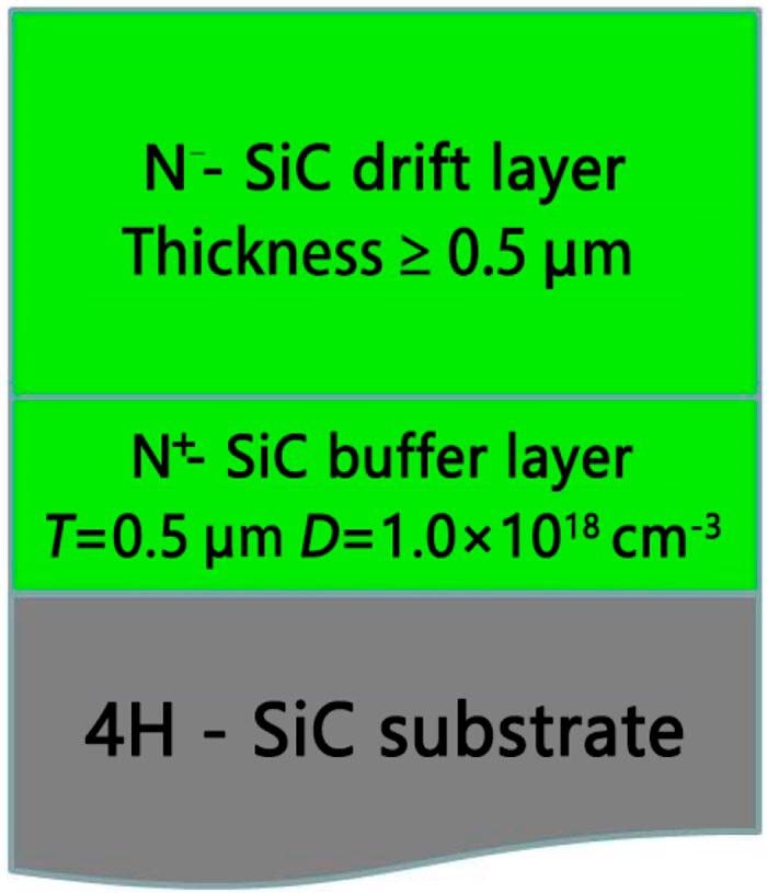 Structure chart of the 4H-SiC homoepitaxial wafer. Image Credit: L. Zhao, Nanotechnology and Precision Engineering
How Doped Homo-Epitaxial Wafers/ Layers are Grown?
The commercial-grade 6-in 4H-SiC homoepitaxial wafer is grown on a 4° off-axis Si-face 4H-SiC substrates using the CVD method. Before the growth of the drift layer, prior surface preparation is carried out through an in-situ etching process using pure H2, SiH4/H2, HCl/H2, or hydrocarbon/H2 at high temperatures, which removes the subsurface damage due to substrate polishing and hence gives regular step structures.
Silane (SiH4), and trichlorosilane (TCS) are used as silicon precursors, and ethylene (C2H4), and propane (C3H8) are usually used as silicon carbon precursors during the growth process. The crucial process parameters that affect epitaxial growth are the growth temperature, pressure, C/Si ratio, and Cl/Si ratio. When the C/Si ratio is too high, surface morphological defects such as triangle defects are easily generated, whereas too low a C/Si ratio causes the formation of severe macro steps and Si droplets on the surface.
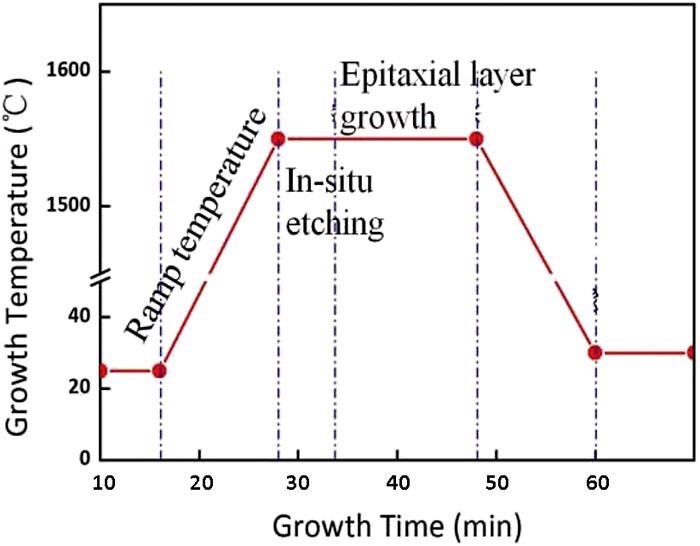
The process sequence of the 4H-SiC homoepitaxial layer using CVD. Image Credit: L. Zhao, Nanotechnology and Precision Engineering
What are the Defects in the 4H-SiC Epitaxial Layer?
The defects in the epitaxial layer cause low breakdown voltage, high leakage current, and poor stability in SiC power electronic devices. The defect is generated during the epitaxial process or extended from the substrate. The typical defects in the epitaxial layer include triangles, pits, carrots, step bunching, dislocations, stacking faults, downfalls, and downfall triangles.
The triangle defect has adverse effects on the yield ratio and reliability of a device. The triangle defects are formed due to the 2D nucleation on terraces, which affects the growth of the step flow. They are of two types viz. acute triangle and obtuse triangle. They can be effectively controlled through the adjustment of the growth process parameters such as the temperature and the C/Si ratio.
The carrot defect increases the reverse leakage current of 4H-SiC Schottky and p–n junction diodes.
The carrot defect consists of ridges. Use of the molten KOH etching method shows that this defect consists of a threading screw dislocation (TSD)-related etch pit as the starting point and a pair of basal plane dislocation (BPD)-related etch pits as the terminating point, and both points are connected by a typical stacking fault intersecting the epitaxial wafer surface. The carrot defect density can be avoided by morphological improvement of the substrate surface under Si-rich conditions.
The surface pits of the epitaxial layer cause a local electric field crowding. They are originated from the threading edge dislocation (TED) and threading screw dislocations (TSD) sites during the epitaxial growth.
They are classified into deep pits and shallow pits. Deep pits have a lateral size of a few μm and a depth of a few nm, whereas shallow pits have lateral size and depth of approximately 1 μm and a few nm, respectively. A lower surface pit density is prepared using a lower C/Si ratio and growth rate.
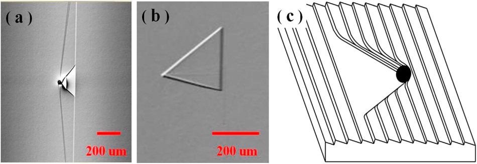
General types (a-b) and formation mechanism (c) of the triangle defect in epitaxial layers. Image Credit: L. Zhao, Nanotechnology and Precision Engineering
Step bunching can induce electric field crowding, resulting in the reduction of blocking voltages. The formation of step bunching on the 4H-SiC epitaxial layer is avoided by precise control of the temperature on the deposition surface during the growth process.
Basal plane dislocations (BPDs) cause performance degradation of bipolar power-electronic devices with a reverse leakage current and forward voltage drift. BPDs are converted to TEDs in epitaxial growth. The conversion effectiveness of BPDs to TEDs can be improved by optimization of process parameters such as interruption growth, buffer process, in-situ etching, and C/Si ratio.
Reference:
L. Zhao, Surface defects in 4H-SiC homoepitaxial layers, Nanotechnology and Precision Engineering, 2020, Vol. 3, Is. 4, p. 229-234. https://aip.scitation.org/doi/10.1016/j.npe.2020.12.001
Disclaimer: The views expressed here are those of the author expressed in their private capacity and do not necessarily represent the views of AZoM.com Limited T/A AZoNetwork the owner and operator of this website. This disclaimer forms part of the Terms and conditions of use of this website.