This has been driven by the remarkable growth in these materials' power conversion efficiencies, with single-junction devices displaying a power conversion efficiency of 25.7%. Perovskite’s band-gap tunability and high compatibility with various processing methods have made it an ideal candidate for use in all-perovskite photovoltaic cells and in conjunction with conventional silicon solar cells.
Recent progress in perovskite-on-silicon tandem solar cells has produced devices with a power conversion efficiency of 29.8%, outperforming all previous perovskite technologies. Metal-halide perovskites are poised to provide the next breakthrough in photovoltaic solar cell technologies, with these devices nearing commercialization.
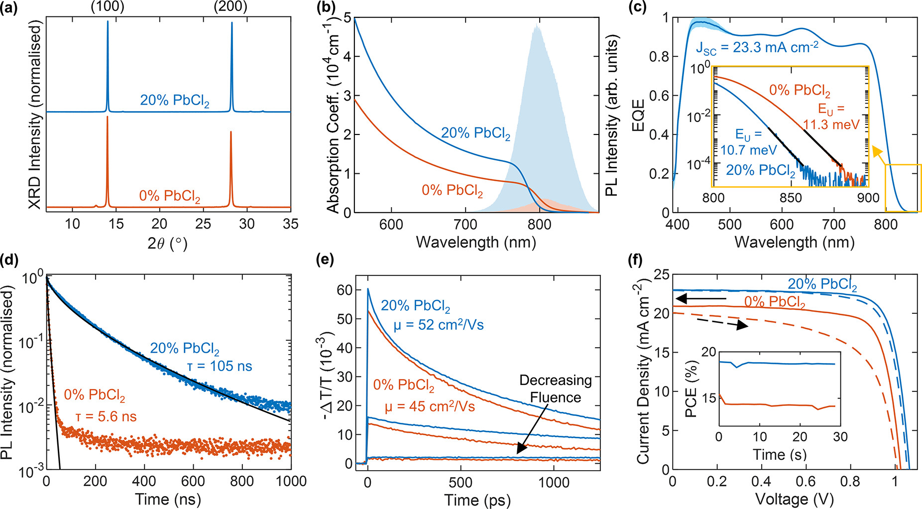
PbCl2 substitution improves device performance. (a) X-ray diffraction (XRD) patterns of FA1–yCsyPb(I1–xClx)3 full photovoltaic devices after testing, grown with (blue line) and without (red line) PbI2 substituted for PbCl2, as denoted in the figure. The XRD patterns were acquired with a Cu–Kα 1.54 Å X-ray source, corrected for specimen displacement, and normalized. (b) Absorption coefficient of bare thin films of the aforementioned composition on z-cut quartz. The shaded region shows the unnormalized PL after photoexcitation at 470 nm. (c) External quantum efficiency (EQE) of a device with 20% PbCl2 and the corresponding integrated short-circuit current (JSC). The inset shows the absorption edge from the EQE and the Urbach tail fit (black line). (d) Time-resolved photoluminescence (PL) traces for thin films of the aforementioned bare films on quartz, after photoexcitation by a 1 MHz pulsed 470 nm laser at a fluence of 20 μJ/cm2. The black line shows a stretched exponential fit. (e) Optical-pump THz-probe (OPTP) photoconductivity transients of the aforementioned bare films on quartz after photoexcitation at 400 nm as a function of fluence (1.0, 10, 42 μJ/cm2). (f) Current–voltage (J–V) measurements of the aforementioned photovoltaic devices under AM1.5 illumination, as measured under reverse bias (solid line) and forward bias (dashed line). The inset shows the power conversion efficiency (PCE) measured at the max power point under continuous illumination over 30 s. Image Credit: Lohmann, K.B et al., ACS Energy Letters
How has this Remarkable Progress Been Possible?
The outstanding results observed in perovskite-based photovoltaic solar cell technologies have been due to remarkable advances in passivation and thin-film crystallization techniques. These techniques have aimed to reduce the semiconducting perovskite layers’ defect density and minimize nonradiative recombination on the surfaces of the materials within their bulk crystals and at interfaces with other materials used in solar cells.
By controlling the precursor phases during thin film deposition and crystallization, thin-film growth can be improved during the manufacture of perovskites. Mixed-solvent systems are typically employed, and this can also be achieved by tuning the solvent lead-halide complexion. Recent research has developed an antisolvent quenching step in processing, which has resulted in improved thin-film quality and reproducibility.
Successful passivation routes have been achieved using processes such as molecular passivation, typically with ammonium or primary amines. Another passivation strategy is to add 2D layered-phase perovskite layers to 3D perovskite films, by either depositing them or mixing the 2D and 3D structured perovskites. Another strategy to enhance crystallization and lead to better optoelectrical properties is to add a small excess of chloride salt to the starting solution.
Developing compatible and industrially scalable manufacturing processes remains challenging, however. Vacuum deposition has been widely explored and shows good promise for the commercial production of metal-halide perovskites. This process is especially attractive for the manufacture of multilayer devices, where sequential deposition of layers of different materials and precise film thickness control is critical.
Whilst there have been advances in vapor-deposited metal-halide perovskites using solutio- processed perovskites, many thin-film control and passivation techniques do not easily translate to dry solvent-free perovskite processing.
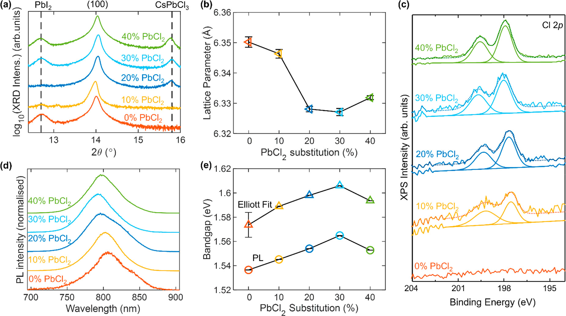
Evidence for incorporation of Cl into bulk FA1–yCsyPb(I1–xClx)3 perovskite. (a) X-ray diffraction patterns of FA1–yCsyPb(I1–xClx)3 full photovoltaic devices after testing, grown with varying amounts of PbI2 substituted for PbCl2, as depicted in the legend. The y-axis shows the logarithm of the measured intensity to be able to show both the large perovskite peak and the much smaller PbI2 and CsPbCl3 peaks. The XRD patterns were acquired with a Cu–Kα 1.54 Å X-ray source. (b) Lattice parameter obtained from the XRD traces in part a for the bulk perovskite fitted to a cubic unit cell. (c) X-ray photoemission (XPS) high-resolution spectra for thin films of the aforementioned compositions deposited on ITO/PTAA, showing the Cl 2p region. (d) Normalized photoluminescence (PL) of the aforementioned bare films on quartz after photoexcitation at 470 nm. (e) Optical bandgap obtained from fits to the PL and electronic bandgap obtained from Elliot fits to the absorption spectra shown in Figure S10 for the aforementioned bare films on quartz. The error bars in parts b and e represent the 1 standard deviation range (68% confidence interval) for the respective fit parameters. Image Credit: Lohmann, K.B et al., ACS Energy Letters
The Study: Investigating the Influence of Elemental Substitution on Perovskites
The authors have investigated the influence of the addition of controlled amounts of chlorine salts during the growth of MA-free perovskite thin films on crystallization and optoelectrical properties. MAI is commonly used as a precursor during vapor deposition processes. This precursor material is hindered by its thermal degradation at low temperatures and inconsistent sublimation behavior.
Four precursors (CsI, FAI, PbI2, and PbCl2) were co-deposited in independently controlled vacuum furnaces in a custom-made vacuum deposition system. The effects of each precursor on the final thin-film perovskites were investigated thoroughly.
It was discovered that substituting different amounts of PbI2 with PbCl2 has a positive impact on both the optoelectronic quality and performance of solar cells. Evidence for retention of chlorine in the final perovskite thin films was uncovered in the study, with the origins of these improvements discussed in-depth.
The most dramatic effect of this substitution was an increase by orders of magnitude of both the quantum yield and lifetime of the perovskite device’s photoluminescence. The photoluminescence of the film prepared with co-deposition of PbCl2 increased to 105 nanoseconds with an eighteen-fold increase.
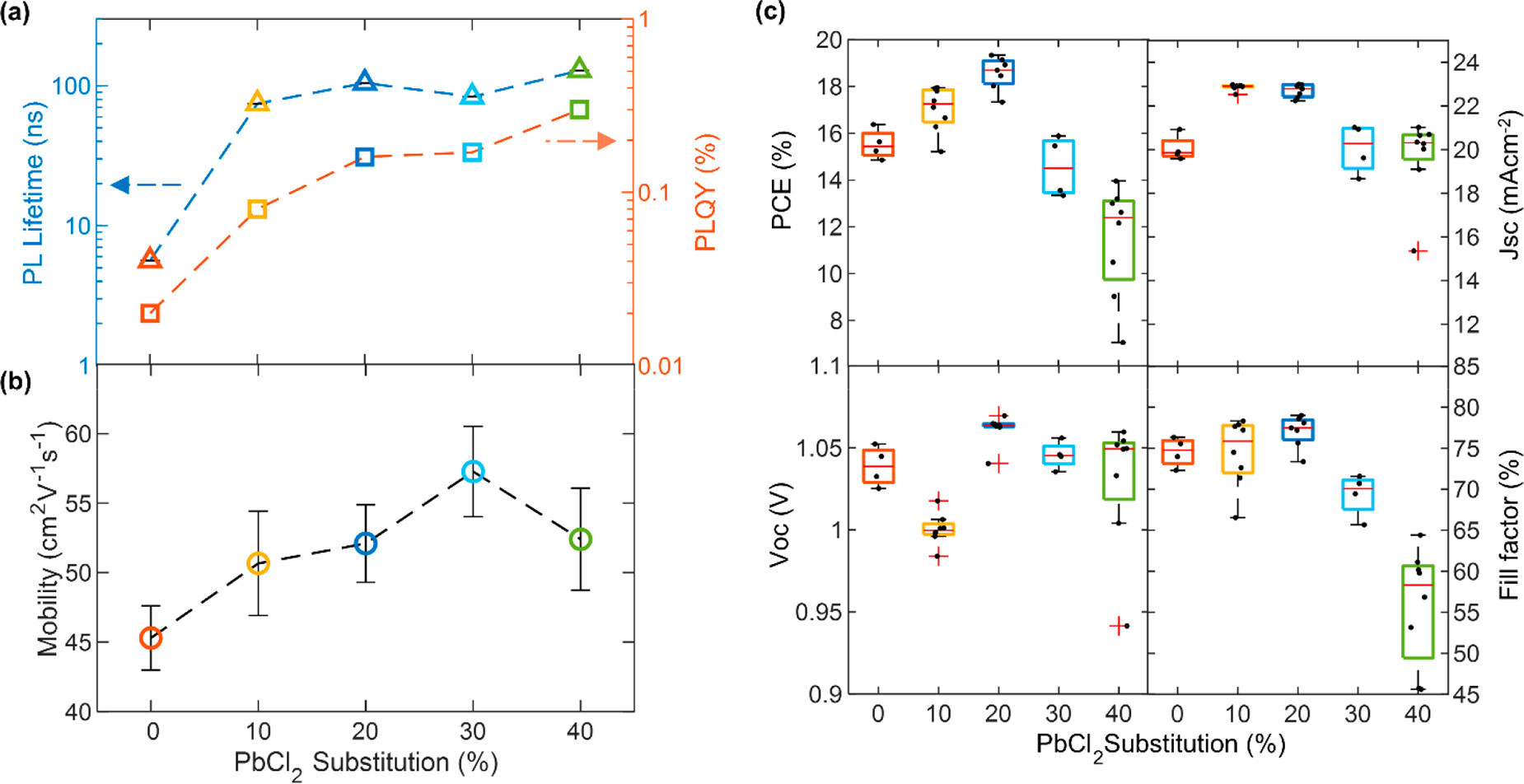
Evidence for defect passivation of FA1–yCsyPb(I1–xClx)3 thin films with Cl addition. (a) Photocarrier lifetimes (blue, left) and photoluminescence quantum yield (PLQY) (red, right) of FA1–yCsyPb(I1–xClx)3 thin films on z-cut quartz, grown with various amounts of PbI2 substituted with PbCl2. The lifetimes were obtained from stretched exponential fits to time-resolved photoluminescence (TRPL) traces, which were obtained by photoexciting the samples with a 1 MHz pulsed 470 nm laser with a fluence of 20 μJ/cm2. The PLQY was obtained through 532 nm photoexcitation at 24 mW cm–2 intensity. (b) Charge-carrier mobilities obtained from optical-pump THz-probe spectroscopy done on the aforementioned bare films. Additional experimental details can be found in the Supporting Information. (c) Current–voltage (J–V) characteristics for reverse scans of 0.25 cm2 and 1 cm2 devices made from the aforementioned FA1–yCsyPb(I1–xClx)3, tested under simulated AM1.5 solar irradiance. The solar cells were made with the following p-i-n structure ITO/PTAA/perovskite/C60/BCP/Ag. Image Credit: Lohmann, K.B et al., ACS Energy Letters
This “dry” solvent-free process developed in the study is compatible with high-volume manufacturing, significantly improving upon previously reported thin-film perovskite processing methodologies. The authors have stated that the strategy in their work can efficiently produce thin films of the highest quality using vapor-deposited methods compared to other reported materials. This will lead to significant improvements in perovskite development in the future.
The paper lays the foundation for incorporating chlorine ions into vapor-deposited perovskite cells. Extending the process’s approach to other metal-halide perovskites such as bromine-based materials will provide further efficiency improvements in the field of perovskite research, opening the possibility of developing efficient and passivated vacuum-deposited multijunction devices.
Further Reading
Lohmann, K.B et al. (2022) Solvent-Free Method for Defect Reduction and Improved Performance of p-i-n Vapor-Deposited Perovskite Solar Cells ACS Energy Letters 7 pp. 1903-1911 [online] pubs.acs.org. Available at: https://pubs.acs.org/doi/10.1021/acsenergylett.2c00865
Disclaimer: The views expressed here are those of the author expressed in their private capacity and do not necessarily represent the views of AZoM.com Limited T/A AZoNetwork the owner and operator of this website. This disclaimer forms part of the Terms and conditions of use of this website.