Innovative, next-generation and high-performance applications such as sensors, RF circuits, transistors, and optoelectronic devices have been developed which take advantage of the numerous excellent properties of graphene.
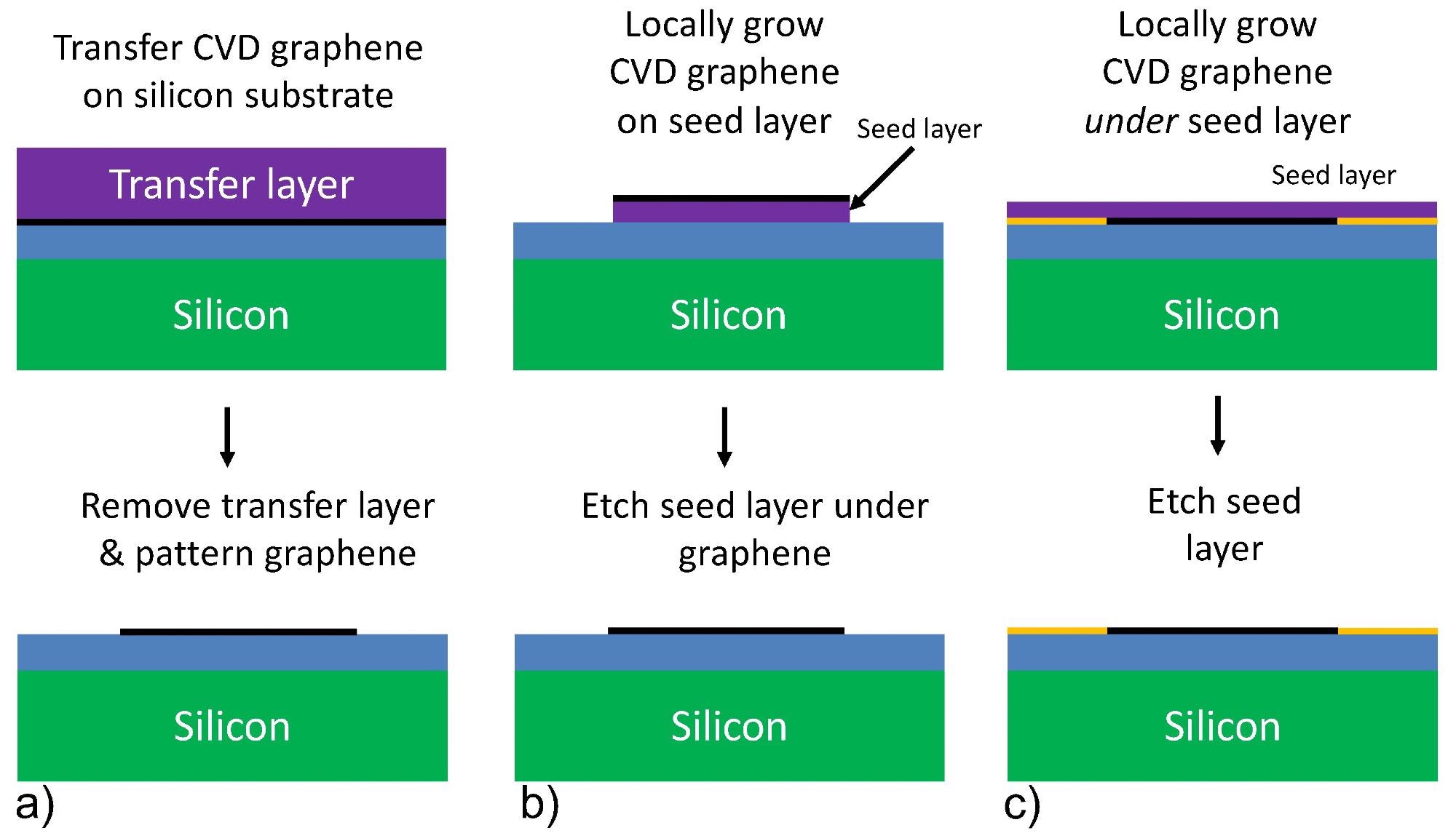
Schematic flows for transfer-based and transfer-free integration of CVD graphene on silicon wafers. (a) Transfer-based integration flow. (b) Transfer-free integration flow, growing graphene locally on top of a seed layer (purple). (c) The focus of this work: transfer-free integration flow growing graphene under a seed layer, where the yellow blocking structure layer is used to define the local graphene growth region. The blue layer in the figure can be the CMOS backend SiO2 layer, or any other interface of choice. Image Credit: Hagendoorn, Y et al., Materials
A key area of research in recent years has been the development of hybrid devices which incorporate graphene and silicon. Incorporating advanced and complementary metal-oxide semiconductors into these hybrid devices is highly desirable.
Manufacturing graphene layers that possess equal dimensions to silicon waters is a key challenge in this research area currently. Fabrication methods that can achieve this urgently need to be developed to realize this integration. Moreover, retaining the quality of deposited graphene layers is essential.
Over the past decade, it has become increasingly clear to scientists that chemical vapor deposition (CVD) is a suitable fabrication process for realizing this goal. Intense research has been conducted in this time period which has highlighted CVD’s benefits as a fabrication route. CVD can produce high-quality and large-area graphene.
Different CVD-based strategies have been explored in recent years for this purpose. Transfer-based integration, where graphene is grown on thin transition metal films, provides substrate-independent optimized graphene growth, protecting the substrate from elevated temperatures, but challenges with this process include imperfections due to polymer contamination.
Transfer-free integration has been developed to address the limitations of transfer-based integration methods. In this process, graphene is directly grown on the substrate, eliminating the transfer process. However, there are limited substrates that can be used. Furthermore, there are limitations in device applications due to the reflectivity and high electrical conductivity of transition metal substrates which are typically used for this purpose.
In recent years, researchers have investigated an alternative approach. This involves using a “seed” layer of materials deposited onto the substrate wafer. Graphene is then deposited onto this seed layer. Transition metals are used, with molybdenum and platinum being the preferred choices in research currently. Etching can then be used to remove the seed layer and produce highly patterned graphene structures that can function as devices such as gas sensors.
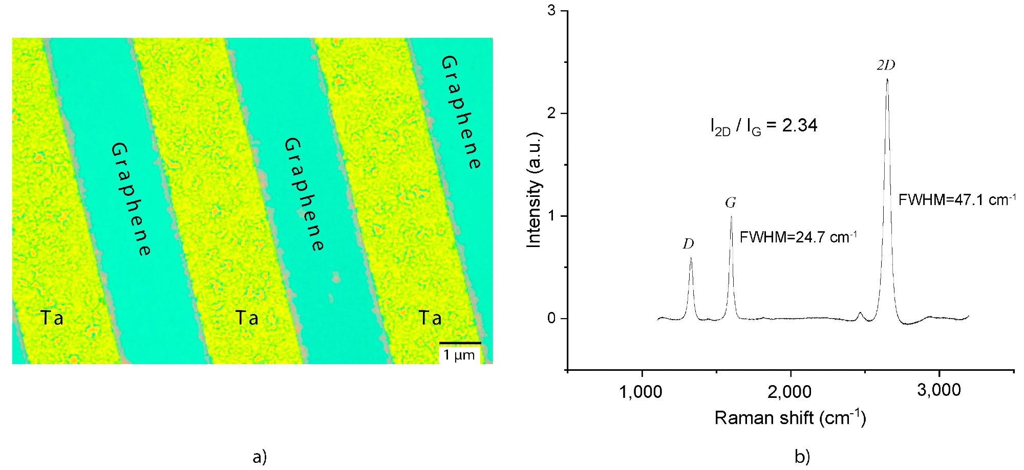
(a) Optical micrograph of a wafer with patterned Ta blocking structures (yellow) and transferless CVD graphene (turquoise). The graphene is grown at the interface between the SiO2 substrate and the Pt seed layer that is removed afterwards. (b) Raman spectrum of CVD graphene layer between Ta blocking structures, yielding Raman peak intensity ratios I2D/IG=2.34 and ID/I2D=0.24 and FWHM2D ≈ 47 cm−1 representative for monolayer graphene. Image Credit: Hagendoorn, Y et al., Materials
The Study
The study in Materials has demonstrated an alternative route for producing graphene on wafer-thin SiO2 substrates. Compared to conventional seed layer approaches, this approach involves growing graphene underneath a platinum seed layer at the platinum/SiO2 interface. This method combines the benefits of transfer-free integration and a seed layer approach to achieve efficient CVD graphene growth on wafer-thin silicon-based substrates.
After localized graphene growth at the interface, the platinum seed layer is removed. The novel fabrication process has several benefits, including reducing mechanical stress, organic contamination, and other challenges which are faced by traditional process flows.
The authors also demonstrated that using an intermediate adhesive tantalum layer between the SiO2 substrate and the platinum seed layer induces localized inhibition of graphene growth. This layer enhances the process by producing patterned graphene layers which can be used in a variety of electronic applications. The authors have noted that similar work was done using an intermediate nickel layer, but this research suffered from the bottleneck of high carbon solubility.
Graphene growth was facilitated at the interface due to the weak bonding between the SiO2 substrate and the platinum layer. At the platinum surface, methane gas is dissociated at elevated temperatures into hydrogen and carbon and is chemisorbed by the platinum catalyst. A highly uniform carbon distribution in the platinum layer is achieved.
The quality and flatness of graphene layer growth on the wafer-thin substrate is possibly facilitated by the lack of surface roughness on SiO2 layers. Moreover, graphene purity may be enhanced due to the diffusion of carbon atoms through platinum.
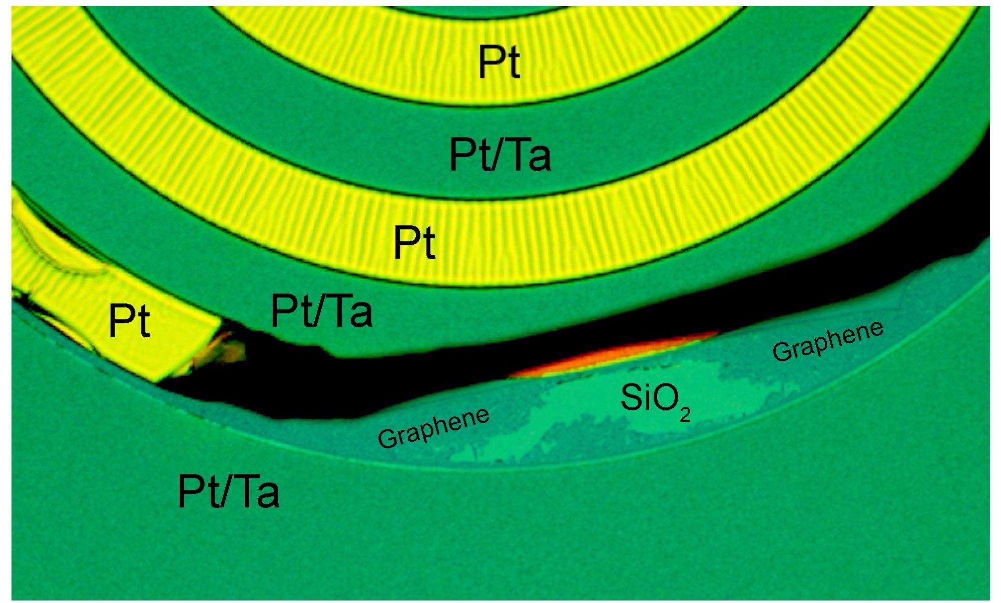
Optical micrograph of a wafer with lift-off patterned Ta structures, after the CVD graphene growth and before the Pt etch process step. Whereas the 50 nm Pt on top of 30 nm Ta is forming a flat surface, with Ta enhancing Pt adhesion, the intermediate regions with Pt show signs of weak adhesion (surface corrugation) and delamination. In a region where the Pt is delaminated, CVD graphene is observed on the SiO2, that corresponds to the graphene in Figure 4 after Pt etch. Image Credit: Hagendoorn, Y et al., Materials
Tantalum and SiO2 bond strongly together, which explains why the growth of the graphene layer is arrested at the tantalum/SiO2 interface along with the low diffusivity of carbon in tantalum. Additional graphene patterning steps are not required using this process. Besides functioning as a blocking layer, the authors have suggested that tantalum could be employed as an electrode in SiO2/graphene-based devices, though this may require additional processing steps.
This novel approach overcomes several disadvantages of current CVD fabrication methods. The authors have stated that tuning the process will provide an innovative route toward producing high-quality and efficient graphene devices for applications such as data processing, high-speed communication, and sensing.
Further Reading
Hagendoorn, Y et al. (2022) Direct Wafer-Scale CVD Graphene Growth under Platinum Thin-Films Materials 15(10) 3723 [online] mdpi.com. Available at: https://www.mdpi.com/1996-1944/15/10/3723
Disclaimer: The views expressed here are those of the author expressed in their private capacity and do not necessarily represent the views of AZoM.com Limited T/A AZoNetwork the owner and operator of this website. This disclaimer forms part of the Terms and conditions of use of this website.