PDs are one of the common optoelectronic devices used extensively in several applications. Functional materials typically used in traditional PDs demonstrate high rigidity, which significantly affects the performance of PDs upon bending or stretching.
Thus, the development of new flexible PDs with foldable and bendable functions has received considerable attention, specifically for the fabrication of implantable, wearable optoelectronic devices.
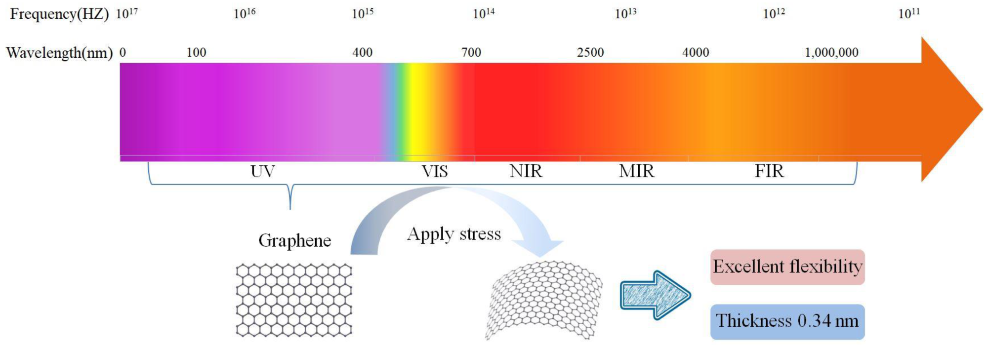
Graphene with exceptional optical and electrical performance deposited on different rigid and flexible substrates as a transparent conductive film has displayed significant potential in PDs. In recent years, several studies were performed to enhance the performance of graphene-based PDs, with a number of them focusing on improving the performance of the graphene conductive films, as these films critically influence the overall performance of the device.
In this study, researchers reviewed the recent developments in graphene-based conductive films for photodetection, all-graphene flexible PDs, and high-performance graphene-hybrid PDs, and discussed the future applications of PDs in flexible wearable electronics.
Bandgap values of various 2D materials and their corresponding detection ranges. Detection range and properties of two-dimensional material graphene. Image Credit: He, L et al., Materials
Transparent Conductive Graphene Films
Graphene-based transparent conductive films used in photoelectric detection must be highly efficient and uniform without agglomeration on the substrate. Chemical vapor deposition (CVD) can be used as an effective technique for the fabrication of large-area graphene films.
Recently, a new CVD technique was developed for the synthesis of a large-area graphene film. The method was different from the traditional CVD processes that require temperatures above 1000 oC for the complete preparation of graphene.
High temperatures can result in the deposition of a large number of amorphous carbon contaminants on the graphene surface, leading to “intrinsic pollution” of the graphene film, which significantly affects the graphene performance.
In this new CVD method, polycarbonate and sapphire are used as substrates, while molten gallium is used as a catalyst. The high-temperature requirement of conventional graphene preparation methods can be eliminated using this method which requires 50 oC temperature to prepare graphene.
Transfer of Transparent Conductive Graphene Films
The transfer of prepared high-quality graphene to the target substrate that is suitable for PDs is essential to achieving large-scale production of graphene films. However, during the transfer process, several impurities are deposited on the graphene film surface, leading to surface contamination that adversely impacts the PD performance. Additionally, the transfer efficiency is reduced during the transfer process as graphene is prone to the formation of defects, folds, or wrinkles.
In the indirect transfer method, a carrier material is used as the supporting layer during the transfer of graphene from the growth substrate to the target substrate, and then the material is removed through chemical or physical methods.
Poly(methyl methacrylate) (PMMA) and polydimethylsiloxane (PDMS) are commonly used as the carrier. High-quality graphene can be obtained using the indirect transfer method through careful selection of the carrier and continued optimization of the transfer process.
In the direct transfer process, graphene is attached directly to the target substrate by peeling off the film from the growth substrate without requiring any carrier material. The graphene film damage rate is reduced significantly in the direct transfer method compared to indirect transfer as cracks are not introduced in the graphene during the degumming process.
However, the adhesion interlayer can adversely impact the graphene performance in the direct transfer process, which can be prevented by directly transferring graphene to the target substrate without using a polymer.
All-Graphene Flexible PDs
The first all-graphene PD was prepared using graphene as a light-absorbing layer. Subsequently, a metal-free low-temperature plasma-enhanced CVD method was used to prepare an all-graphene PD with a high detectivity and response rate in the visible range.
However, graphene has a limited external quantum efficiency (EQE) and light absorption capacity as it lacks a bandgap and absorbs the entire electromagnetic spectrum owing to its very low light absorption coefficient.
Heterostructure recombination, resonant cavity enhancement, and plasma enhancement can be used to improve the graphene PD performance. An integrated waveguide PD fabricated using metal-doped graphene demonstrated wide spectral bandwidth, high speed, and high responsiveness. The device responded uniformly under 1450 to 1590 nm illumination. Such graphene hybrid PDs based on heterogeneous recombination or doping display significantly improved specific detectivity and light responsivity.
Graphene Hybrid PDs
Halide Perovskite-Type Graphene Heterostructure PDs
Perovskite materials display superior light absorption characteristics. For instance, the cesium lead halide (CsPbX3) perovskite nanocrystal photoluminescence is characterized by 1–29 ns radiative lifetimes, high quantum yields of 90%, extensive color gamut that covers up to 140% of the National Television Standards Committee (NTSC) color standard, and narrow emission line widths.
Halide-type perovskite materials were specifically investigated as high-efficiency light-absorbing materials in optoelectronic devices due to their excellent optical properties. In a study, a flexible perovskite/graphene hybrid channel field-effect phototransistor structure was prepared and evaluated. The fabricated phototransistor displayed a highly sensitive and narrow light response over the visible spectrum.
All-Carbon PDs
Semiconductor C60, a type of low-dimensional carbon material, displays considerable absorption from the ultraviolet (UV) to the near-infrared (IR) regions. The medium bandgap C60 prevents the photoelectric detection of low noise and allows the suppression of dark current observed in graphene due to the lack of bandgap.
This carbon material can be used in several applications in low-cost flexible optoelectronic devices as it possesses exceptional mechanical and optoelectronic properties. Thus, the combination of graphene and C60 can overcome the drawbacks of all-graphene PDs, while the unique semiconductor characteristics of C60 can improve the performance of all-carbon flexible PDs.
Single-walled carbon nanotubes (SWCNTs) can also be used to fabricate high-performance all-carbon PDs due to their high mobility and an on/off ratio of 105. For instance, SWCNT-graphene heterostructure-based thin-film transistors can operate under 20% strain while displaying very high transparency and high mechanical strength.
Graphene/Transition Metal Halide Heterostructure-Based PDs
Atomically thin vertical heterostructures displayed considerable potential in optoelectronic applications owing to their transparency and flexibility. Two-dimensional (2D) transition metal dichalcogenides (TMDs), specifically layered materials with weak out-of-plane bonding, strong in-plane bonding, exceptional photoelectric properties, and mechanical flexibility, are typically used to fabricate these heterostructures.
These layered materials with a narrow bandgap and high carrier mobility demonstrate robust light-matter interactions. Thus, the stacking of these 2D material crystals with extensive optical properties and graphene can facilitate the synthesis of high-performance optoelectronic devices.
Among the TMDs, molybdenum disulfide and tungsten disulfide were investigated extensively for applications in optoelectronic devices to fabricate graphene/transition metal halide heterostructure-based PDs as they display high chemical stability and have an energy gap in the visible region of the electromagnetic spectrum.
Application of PDs in Flexible Wearable Electronics
A flexible PD can be placed on the skin surface to form a wearable patch to monitor human health. Similarly, a photoelectric device composed of an ultrathin neural-interfacing electrode (UNE) and a curved image sensor (CurvIS) array was developed by imitating the structural characteristics of the human eye and using an anatomically thin molybdenum disulfide-graphene heterostructure softly implanted into the human eye retina.
The responsivity of the heterostructure device was substantially higher compared to silicon photodiodes of a similar thickness, which indicated its great potential for use in biomedical applications. Similarly, a new type of wearable paper-based PD was recently fabricated that can measure the dose and intensity of UV light simultaneously. Moreover, the photoelectric signal remained stable even after 1000 bends.
Conclusions and Future Outlook
Graphene flexible PDs have significant development prospects in the Internet of Things and wearable devices as graphene can be used as both a light-absorbing layer and transparent conductive layer.
Moreover, graphene can be combined with different materials to improve the sensitivity of the resulting PD and extend its detection spectrum from UV to mid-IR bands. Graphene PDs can also be used for other sensing elements, such as biosensors or gas sensors, to realize multifunctional sensing.
However, more research is required to thoroughly study the charge transfer in heterojunctions and to improve the overall PD performance. Moreover, the cost and complexity issues of the existing graphene film preparation methods must be addressed in the future.
Disclaimer: The views expressed here are those of the author expressed in their private capacity and do not necessarily represent the views of AZoM.com Limited T/A AZoNetwork the owner and operator of this website. This disclaimer forms part of the Terms and conditions of use of this website.