Lightweight and flexible thin film SCs have received significant attention as a power source for foldable, bendable, and stretchable electronic devices. Perovskite, chalcopyrite, and crystalline silicon (c-Si)-based flexible SCs are typical examples of bending tolerant highly efficient photovoltaic devices (PVs).
However, kesterite materials that are abundant on Earth, including Cu2ZnSn(S,Se)4 (CZTSSe), Cu2ZnSnSe4 (CZTSe), and Cu2ZnSnS4 (CZTS), are considered a more suitable alternative to perovskites and c-Si owing to their low cost and non-toxicity.
Kesterite materials possess a high absorption coefficient of 104 cm−1, and their band gap can be tuned from 1.0-1.5 eV by adjusting the sulfur/selenium (S/Se) ratio. Kesterite CZTSSe thin-film SCs have achieved a 12.6% power conversion efficiency (PCE) when fabricated using a two-step non-vacuum hydrazine-based fabrication process and 12.62% PCE when fabricated using the sputtering process.
A 12.5% PCE was realized when CZTSe thin film SCs were fabricated through metallic precursor sputtering. However, kesterite materials possess a narrow phase stability, which leads to the formation of defects and secondary phases that adversely affect the PV performance/PCE.
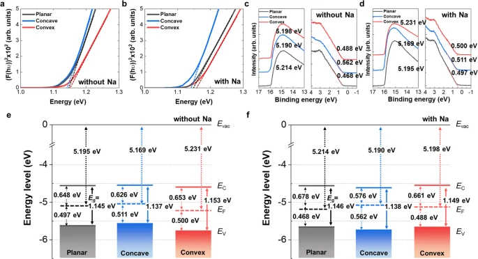
Changes in electronic band structure with mechanical stress. a, b Tauc plot obtained from diffuse reflectance spectroscopy (DRS). c, d Valence band edge and work function of CZTSSe (c) without and (d) with Na elements under planar, concave, convex bendings. e, f Schematic band diagram of CZTSSe (e) without and (f) with Na elements under planar, concave, convex bending states. Evac, EF, EC, and EV are vacuum, Fermi, conduction, valence level, respectively. Image Credit: Park, H.K et al., npj Flexible Electronics
Several studies have demonstrated the feasibility of using alkali dopants to suppress intrinsic defect formation. Additionally, artificially doping alkali elements in a flexible substrate can effectively improve SC efficiency.
Specifically, the use of sodium as a dopant and optimization of doping conditions can significantly increase the efficiency of flexible thin film CZTSSe SCs. For instance, flexible CZTSSe SCs with an extra sodium fluoride (NaF) doping layer displayed a PCE of 11.19%.
Understanding the changes in optoelectronic characteristics of thin film CZTSSe SCs induced by mechanical stress under different bending conditions is crucial for the long-term and large-scale application of flexible CZTSSe devices to non-flat surfaces.
The Study
In this study, researchers investigated the effect of sodium doping on the carrier transport mechanisms and the electronic band structure of flexible CZTSSe PVs under mechanical stress at concave and convex bending conditions. Flexible CZTSSe PVs with a tin/copper/zinc (Sn/Cu/Zn) stacking order were fabricated on a molybdenum (Mo)-coated Mo-foil substrate without and with an additional NaF layer.
The CZTSSe thin-film SC was composed of a 0.1-mm-thick Mo-foil substrate, CZTSSe absorber fabricated through sputtering, 50-nm cadmium sulfide (CdS) buffer layer deposited using chemical bath deposition, 50-nm intrinsic zinc oxide (ZnO) layer deposited using radio-frequency (RF) sputtering, 300-nm aluminum (Al)-doped ZnO (AZO) layer/transparent conducting oxide deposited through sputtering, and 500-nm Al collection grid deposited using thermal evaporation.
Among the five fabricated precursor structures, four structures contained an additional NaF layer at different metallic-precursor stack positions. These structures include NaF/Sn/Cu/Zn/Mo/Mo foil, Sn/NaF/Cu/Zn/Mo/Mo foil, Sn/Cu/NaF/Zn/Mo/Mo foil, Sn/Cu/Zn/NaF/Mo/Mo foil, and Sn/Cu/Zn/Mo/Mo-foil, which were designated as CZTSSe5, CZTSSe4, CZTSSe3, CZTSSe2, and CZTSSe1, respectively.
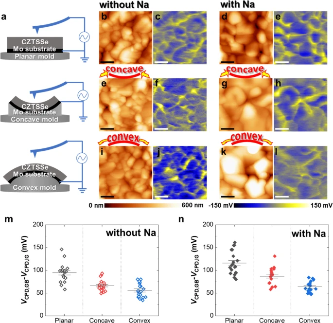
Distribution of contact potential difference in various bending modes. a Diagram representing the KPFM setup in the planar and bending modes. b–l Surface topography (b, d, e, g, i, k) and contact potential difference (VCPD) map (c, e, f, h, j, l) of Na-undoped and doped CZTSSe absorber material in the planar state and the concave and convex bending modes with a bending radius of 20.47 mm. (scale bar: 1 μm) m, n Distribution of VCPD difference between the intra-grain (IG) regions and grain boundaries (GBs) of Na-undoped (m) and doped (n) CZTSSe absorber material in the planar state and the concave and convex bending states. The CZTSSe absorber doped with Na displayed greater carrier separation at the GBs than the CZTSSe absorber without Na. Image Credit: Park, H.K et al., npj Flexible Electronics
The Mo back contact layer was coated on the Mo-foil substrate, while Zn, Sn, and Cu of 99.99% purity were used for metal-precursor sputtering. A 10-nm NaF layer was deposited using the thermal evaporation method during the fabrication of four precursor structures with a NaF layer. The metallic precursors were sulfo-selenized using Se pellets as the Se source and diluted hydrogen sulfide gas with 90-vol% argon as the S source in a rapid thermal process (RTP) chamber.
Ultraviolet (UV)-visible-near infrared (NIR) spectroscopy, UV photoelectron spectroscopy (UPS), photo-assisted Kelvin probe force microscopy (KPFM), and amplitude modulation (AM)-mode KPFM measurements were performed to characterize the synthesized samples. A homogeneous strain was applied to the fabricated samples by attaching them to bending molds during the UPS and UV-visible-NIR measurements.
Mechanical stress was applied to the fabricated flexible CZTSSe thin-film SCs by bending the samples and then local electrical characteristics were analyzed to evaluate the changes in carrier behavior and charge barriers at the bent material surface. The local open circuit voltage (VOC) loss in the bending mode was also investigated using the carrier excitation mechanism.
Additionally, researchers evaluated the photovoltaic parameter degradation due to the concave/convex bending. During the bending test, the PV device parameter values were obtained after 1000, 800, 600, 400, and 200 bending cycles at 50 mm bending radii. Convex and concave bending were applied to the fabricated SCs at 1.0 mm s−1 speed.
Significance of the Study
Flexible and highly efficient CZTSSe PVs with and without NaF layer were fabricated successfully. The CZTSSe electronic structure was deformed under stress due to the changes in work function, valence band edge, and band gap.
The electron barrier height of the CZTSSe absorber layer reduced under mechanical stress, and the carrier separation weakened at grain boundaries, leading to carrier recombination. Less-degraded carrier transport was observed in sodium-doped CZTSSe devices compared to undoped CZTSSe devices.
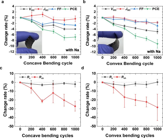
Changes in photovoltaic device parameter by mechanical bending test. a, b Rate of change of photovoltaic device parameters with concave (a) and convex (b) bending with a bending radius of 50 mm and a maximum of 1000 bending cycles. Photovoltaic device parameters were measured after 200, 400, 600, 800, and 1000 bending cycles. The inset in (a, b) shows an image of the bent device. c, d Rate of change of series and shunt resistance with concave (c) and convex (d) bending with the same bending condition. Error bars in (a–d) are defined as standard deviation of photovoltaic parameters obtained from four points of two devices. Image Credit: Park, H.K et al., npj Flexible Electronics
Moreover, the CZTSSe band gap increased and decreased in the convex and concave bending states, respectively. The upward/downward shift in the Fermi level in the mechanical bending states affected the band alignment.
The local VOC on the bent CZTSSe surface reduced due to limited carrier excitation. The reduction in local VOC was higher during convex bending than concave bending, indicating a greater charge carrier recombination under the convex bending state. The loss of local VOC under mechanical stress was consistent with the significant reduction in device Voc during both concave and convex bending tests.
To summarize, the findings of this study demonstrated that the carrier transport degradation in flexible thin film CZTSSe SCs was higher in the convex bending state compared to the concave state. Moreover, the insight gained in this study can help in understanding the stress-induced optoelectronic changes in other flexible PVs, such as perovskite and silicon SCs.
Disclaimer: The views expressed here are those of the author expressed in their private capacity and do not necessarily represent the views of AZoM.com Limited T/A AZoNetwork the owner and operator of this website. This disclaimer forms part of the Terms and conditions of use of this website.