Vitrek announced today that its Proforma 300iSA semi-automated metrology system has proven capable of supporting wafer inspection across a growing range of semiconductor materials, wafer sizes, and surface finishes including silicon (Si), silicon carbide (SiC), gallium arsenide (GaAs), and indium phosphide (InP).
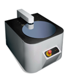 Image Credit: Vitrek
Inspection systems are being pushed to handle more various materials and tighter processes as device manufacturers move beyond traditional silicone into compound semiconductors for power electronics, RF devices, and photonics. Market analysts project the semiconductor metrology and inspection equipment sector will more than double from approximately $11 billion in 2025 to over $23 billion by 2029, a trend driven by the need to handle an increasing variety of semiconductor types and more precise process nodes.
The Proforma 300iSA is proven capable of inspecting both semiconducting and semi-insulating wafers made from a variety of materials and wafer diameters from 76 mm to 300 mm. Moreover it can be used across process stages as it is compatible with cut, lapped, etched, polished, and patterned surfaces.
"The industry is shifting rapidly toward heterogeneous materials," said Dan Melchior, Semiconductor Test Product Manager at Vitrek. "The Proforma 300iSA provides a single platform that can help manufacturers maintain inspection consistency while reducing complexity on the production floor."
The automated full-scan capability of the system improves inspection throughput while reducing operator variability. Its configurable workflows and user interface allow manufacturers to remotely adapt inspection parameters by process step, lot, or supplier, supporting both R&D environments and high-volume production lines.