Vitrek, a US-based leader in precision measurement instruments, today announced the expanded capabilities of its MTI Accumeasure Capacitance Technology. Designed to make high-precision wafer metrology more accessible to start-up and smaller niche semiconductor equipment makers, Vitrek's Accumeasure technology provides a compact, cost-effective alternative to traditional high-end optical systems that are often too bulky or expensive for new market entrants.
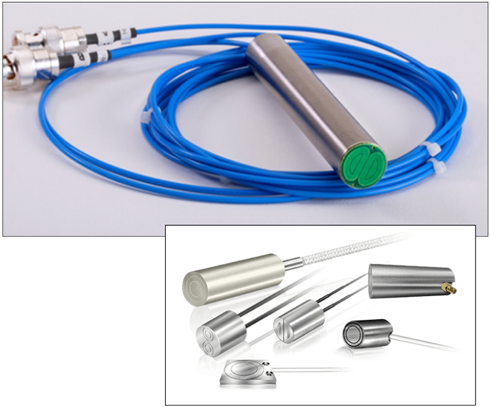 Image Credit: Vitrek
Key segments benefiting from more flexible manufacturing capabilities include MEMs, military, and custom ASIC producers, where volumes are typically lower. Accumeasure technology is also Why Small Fab And Assembly Houses Are Thriving well-suited to the needs of the growing number of small-volume mini-fabs that can launch operations with less than $200 million in capital investment. These facilities can economically manage small run volumes and process wafers in under one inch in diameter, compared to the 6-12-inch wafers commonly used in large-scale fabs.
According to Future Bridge Americas, an organization focused on empowering North American industries through strategic events, "Mini semiconductor fabs are revolutionizing semiconductor manufacturing as viable alternatives to massive plants."
Achieving high precision and enabling faster changeover times helps mini-fabs pursue higher-margin projects and strengthen market differentiation. "Silicon R&D does not typically follow a 'prototype here, production there' model," said Samer Bahou, Director of Marketing Communications at SEMI, in a recent article. Production can also be more manageable with a steadier stream of smaller wafers rather than shorter runs of larger wafers.
This is where Vitrek's non-contact Accumeasure system excels. Its proprietary probes are available in custom sizes and offer 0.1 nm resolution (24-bit) with linearity limits beyond ± 0.01 % FSR. The companion Accumeasure D two-channel measurement system is available in DIN-rail, table-top, and PC-card versions. These rugged boxed units are smaller than a standard 3.5" hard driven enclosure (46 mm x 106 mm x 62 mm).
Different applications require different metrology approaches, noted Dan Melchior, Semiconductor Product Manager at Vitrek. "Our goal is to provide manufacturers with cost-effective access to the precision measurement capabilities needed for specific and also modular applications, helping them achieve measurements that far exceed ASTM and SEMI standards. And we have systems in prototype that go beyond what our current systems can deliver."
Optical interferometer and ellipsometry systems, while extremely precise, require significant capital investment, specialized infrastructure, and extensive operator training. These requirements have driven increased demand solutions like the Vitrek Accumeasure, which integrates with NI LabVIEW™ and enables start-ups to implement in-house quality control at a reasonable cost.
The CHIPS Act allocated $52.7 billion to support revitalization of the domestic semiconductor industry, according to the National Institute of Technology (NIST). A key objective is strengthening the security and resilience of the semiconductor supply chain. "This is where Vitrek's U.S.-developed and U.S.-manufactured technology should provide especially strong value," Melchior added. Our Accumeasure market is strong overseas. With the incentives out there, we are hoping to deliver increasing value to US companies as the US market grows and diversifies.