A precisely focused burst of extreme ultraviolet light can reshape silicon in a single shot, raising new questions about how far maskless semiconductor machining can go.
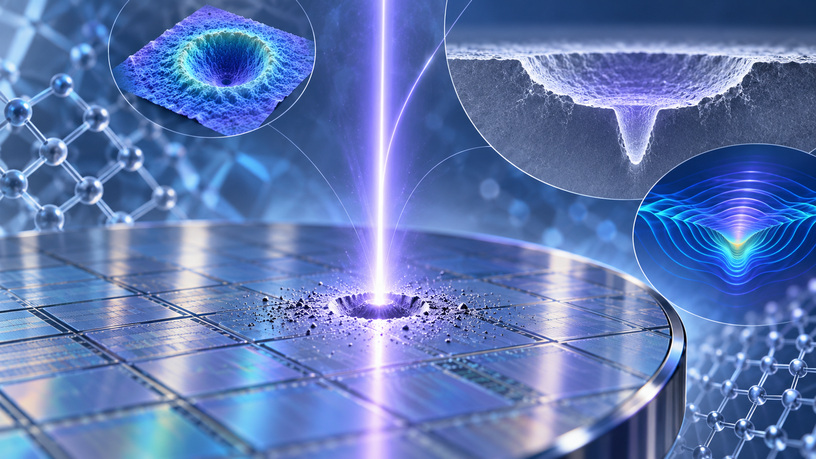
Paper: High-precision machining of silicon surface with intense femtosecond extreme ultraviolet pulses. AI-generated abstract conceptual image created using ChatGPT/OpenAI
*Important notice: This news reports on an unedited version of an accepted paper and is awaiting final editing. Therefore, the paper should not be regarded as conclusive or treated as established information.
In a recent Scientific Reports study, researchers demonstrated a proof-of-concept approach for high-precision machining of silicon surfaces using single extreme ultraviolet (EUV) laser pulses. They used 30-femtosecond free-electron laser (FEL) pulses with a photon energy of approximately 92 eV to create craters up to 1.8 µm deep. Most craters were micrometer-scale, though the lowest dose achieved sub-micrometer widths.
The results demonstrate controlled surface removal and support the prospect of maskless direct writing. The authors expect ultrashort pulses to limit thermal damage, but this was not measured directly.
Limits of Conventional Semiconductor Patterning
Semiconductors, such as crystalline silicon, are central to modern electronics and clean energy systems. As circuits shrink, EUV lithography has emerged as a key method for fabricating fine semiconductor patterns. But this technique relies on complex, defect-free reflective photomasks that are costly and difficult to produce.
Laser direct writing (LDW) offers a mask-free alternative, using focused laser pulses to remove surface layers. Conventional visible and near-infrared lasers face diffraction limits that restrict the smallest features they can create. Thermal effects and rapid energy dissipation can also cause unwanted damage to the substrate, including stress and microcracking.
Using EUV wavelengths for direct writing could help overcome these limits by enabling finer surface removal while reducing heat-related damage.
Experimental Setup and Simulation Methodology
To understand how pulses interact with semiconductor substrates, researchers conducted experiments at the SACLA facility in Japan. They used 92 eV photons to strike a 525 µm-thick silicon wafer at normal incidence. At this wavelength, silicon has near-zero reflectivity and an attenuation length of 0.59 µm.
A two-stage optical system, including a Kirkpatrick-Baez pre-focusing mirror and an ellipsoidal mirror, focused the beam to dimensions of 350 × 700 nm. The researchers irradiated silicon samples mounted on precision stages with single pulses at various positions.
The study also employed a multiscale simulation system called SURFwiX (Surface processed with X-rays).
The XTANT atomistic code modeled electronic excitation and non-thermal changes during the initial femtosecond-to-picosecond stage. LAMMPS molecular dynamics simulations then modeled silicon deformation, pressure-wave propagation, and ablation over picosecond-to-nanosecond timescales. These simulations used Tersoff and Stillinger-Weber interatomic potentials.
To make the molecular modeling feasible, researchers applied the principle of similitude, scaling down the simulated dimensions while maintaining the same absorbed dose.
Dose-Dependent Crater Formation and Characteristics
Atomic force microscopy (AFM) showed that crater size and shape depended on the absorbed radiation dose. At 8 eV per atom, equivalent to a surface fluence of 6.0 J/cm², single EUV pulses produced craters with average depths of nearly 1.5 µm.
Most craters had a broad upper bowl that narrowed into a central dip, reaching depths of up to 1.8 µm; one analyzed crater instead showed a pronounced rim of redeposited material. Their sizes varied by about 13% to 20% across repeated shots.
At 5 eV per atom (3.7 J/cm²), the craters averaged 1.0 µm deep and 1.1 µm wide. Width deviations were about 10%, while depth deviations ranged from 18% to 36%. At the lower dose of 2 eV per atom (1.5 J/cm²), ablation remained largely confined to the primary optical absorption zone, resulting in craters nearly 0.6 µm deep. These craters followed the sub-micrometer laser spot more closely, but their bottoms were rougher and contained unablated silicon fragments.
Molecular dynamics simulations reproduced the dose trend but underestimated crater sizes by about a factor of 3 in depth and 2 in width at 8 eV per atom. They also suggested that silicon near crater edges partially fell back and solidified after ablation, which may contribute to rim formation.
Potential Manufacturing Applications
Maskless EUV LDW could have practical uses in semiconductor manufacturing. Conventional photomask production is resource-intensive, involving resist coating, electron-beam exposure, chemical baths, plasma etching, and resist stripping. EUV LDW could combine these steps into a dry process that uses fewer resources and has lower environmental impact, though those benefits were not measured.
With focused spot sizes on the order of several hundred nanometers, the technique may suit photomasks for larger-geometry integrated circuits used in MEMS sensors, motor control, battery management, and medical devices.
Beyond silicon, the paper cites prior EUV work on thin nickel films and polymers and points to silicon nitride photonic chips as another possible application. Further testing is needed to assess processing rates and performance across other substrates.
Compact EUV Sources for Broader Adoption
The study showed that single femtosecond EUV pulses can machine silicon reproducibly, with most craters remaining micrometer-scale and sub-micrometer width achieved along one beam axis at 2 eV per atom. The approach was validated at a free-electron laser facility; broader adoption could be aided by compact EUV sources, with high-harmonic generation (HHG) as one candidate.
The authors suggest that attosecond EUV pulses could further suppress thermal stress. The mismatch between simulations and measurements suggests that atomistic models need improvement, and manufacturing throughput and environmental benefits remain untested.
Disclaimer: The views expressed here are those of the author expressed in their private capacity and do not necessarily represent the views of AZoM.com Limited T/A AZoNetwork the owner and operator of this website. This disclaimer forms part of the Terms and conditions of use of this website.