 Interview conducted by Courtney Garner, MAFeb 6 2020
AZoMaterials spoke to Dr. James Trevey, CTO of Forge Nano, about how atomic layer deposition works, how the technology is maturing, and how it can be commercially adopted.
Could you give our readers some background on Forge Nano and the solutions you offer?
Forge Nano was originally established as a holding company for intellectual property developed during the founder’s tenure at the University of Colorado Boulder. After receiving some government funding the company formally established itself in 2013 with a commercial address.
The core focus of the company was on commercializing Atomic Layer Deposition (ALD). ALD is an elegant surface engineering technique, the crème de la crème of deposition methods for surface science, that has existed for over 60 years. However, at the time Forge Nano was founded, ALD was stuck in a realm of university-designed student-built systems and low-level proof-of-concepts. The only place for ALD, prior to Forge Nano, was in research articles.
Fluidized beds are the fundamental technology that makes ALD possible. But while they are amazing tools for doing R&D, they are prohibitively expensive to scale. As a result; the general understanding in the field has been that, while the technology is great for improving material properties, it is just too expensive.
Forge Nano came up with a solution to this problem: we took the time-based process of the fluidized beds and turned it into a spatial process. In this spatial process many batches of material can be processed simultaneously by a single instrument, as opposed to the single batch limits of the fluidized bed, enabling a continuous and automated workflow fit for a commercial environment. This innovative concept was the first step towards commercializing ALD for particles and just about anything for that matter.
Could you explain how the process of Atomic Layer Deposition works?
The process behind ALD is implicit in its name: it is where a single atom at a time is deposited onto a surface until a complete layer is formed. Layers are formed by “precursors” which are added sequentially. The process is self-limiting by nature of the precursors involved: The first precursor will bind to all available sites on the surface, but can’t continue building on itself; resulting in a 1-atom thick covering.
The next step in the process is to introduce a second precursor which can react with the layer of the initial precursor which has bound to the surface. This second precursor behaves in the same self-limiting way and completes a fully formed layer with an intended surface chemistry. From there, one can repeat the addition of layers to build a coating of a desired thickness. As an example, Al2O3 is a popular ALD coating and "grows” at ~1.1 Angstroms per layer. Therefore, it takes 9 repetitions of this layer to build a ~1 nanometer thick coating around the substrate of interest.
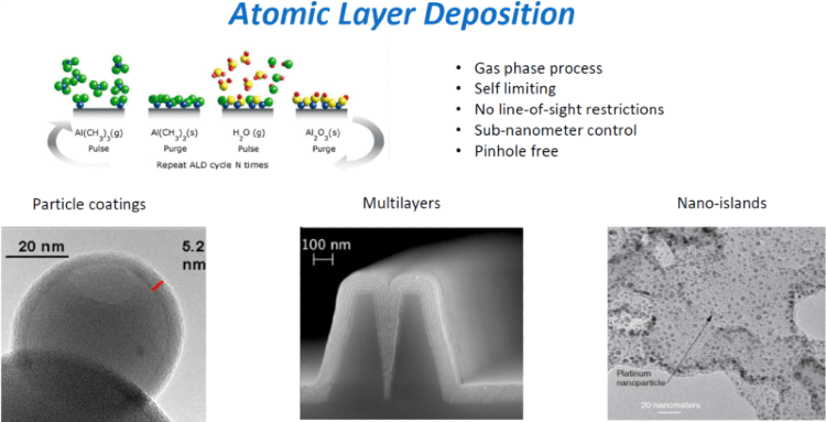
Image Credit: Forge Nano
What does this process achieve?
Imagine an M&M and a hunk of chocolate sitting on the sidewalk in the summer heat. If you were to walk away for a few hours and come back, you would return to a melted mess and an M&M. The M&M survived because of its shell. ALD applies that shell, but to any material, and not just for thermal protection, but many others benefits such as flowability, conductivity, and reactivity.
What are the common applications of particle Atomic Layer Deposition?
ALD is most widely known in semiconductors. It is broadly accepted and has likely been used to make just about any consumer electronic device you can imagine. This stems from the technique’s unique ability to create wonderfully conformal and reliable coatings, with controllable thickness, on whatever it touches. Semiconductors have come a long way in the past decade thanks to ALD. Beyond semiconductors, again, it is still broadly considered to only be an expensive lab-scale technique for improving materials, with no merit beyond proof of concept. Since Forge Nano came to be, there are many applications which are blossoming in the space including:
- Li-ion Batteries - where ALD can be used to increase battery lifetime, energy density, power density, and safety
- Catalysts – where ALD improves reactivity, lifetime, recyclability, and lowers production costs
- 3D Printing – where ALD enables new alloys, improves flowability, reduces oxidation, and increases printing efficiency.
There are many more areas and applications such as pharmaceuticals, cosmetics, and magnetics: the list is endless.
Image Credit: Forge Nano
Could you tell our readers about how Forge Nano creates laboratory-scale ALD coatings?
Forge Nano maintains a staff who, combined, have over 200 years of ALD experience. That experience allows us to scope new projects and assess commercial viability. As ALD is so widely applicable, it is important for Forge Nano to focus on projects which we believe to show commercial promise. While we allocate a small amount of resources to special cases of interest, most of our work must be focused and strategic to achieve our goal of commercialization.
We apply coatings at lab-scale using our commercially available lab-scale tools called Prometheus. Prometheus is the culmination of numerous years and iterations of building fluidized beds and using them. We supply the Prometheus systems to other research organizations because there is no way we can do all of the research and development in the world – nor do we want to! We specialize in scaling, and our goal is to achieve as much as possible.
We load materials into reactors, apply the correct sequence of pre-specified precursors for the correct number of iterations, as determined by the scope and goal of a project. We characterize our coatings physically to ensure they meet our expectations and, when necessary, evaluate them in an appropriate application-based method.
How are these coatings used in research and development applications?
Typically, coatings at the R&D scale are used for proof-of-concept. The goal at this stage is simply to perform an apples-to-apples comparison of ALD-coated materials against the uncoated materials, in a simple and often application-specific manner, which demonstrates compelling data in favor of ALD. Upon success of proof-of-concept testing, the speed and scale of the next steps depend heavily upon the risk tolerance of the interested party.
 Image Credit: Forge Nano
How does Forge Nano apply manufacturing principles to Atomic Layer Deposition?
Forge Nano is the first to apply manufacturing principles in this space. The concepts of all initial designs and prototypes were derived from Design For Manufacturing (DFM) principles. This includes concepts such as keeping things simple, minimizing moving parts, and using as many off-the-shelf parts as possible for the system to keep costs down.
As our systems mature, Forge Nano continues to pursue improvements with DFM principles in mind. Regarding the productization of ALD-coated materials, our methods stem from the six-sigma method known as DMAIC – which stands for Define, Measure, Analyze, Improve, Control – in conjunction with strict management of change (MOC) protocols. Utilizing these basic methods during our scaling efforts ensures that our product development efforts are focused, and produce repeatable and reliable results.
Are there any challenges associated with scaling up for manufacturing-scale powder ALD?
There are many challenges. One challenge we face is differentiation between materials. It is important to differentiate not just between, say, a magnetic powder and a catalyst powder; but even between supposedly identical materials produced by different manufacturers. For example, a Li-ion cathode powder known as NMC811 made in Germany could behave completely differently to one made in China; even though it is supposed to be the same basic material. This is why we are so focused on finding partners with whom we can focus on a single material or performance specification, and spend our time doing product development vs. just proof-of-concept tests.
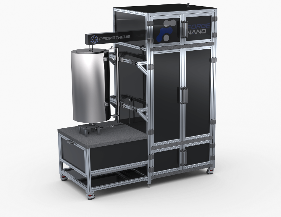
Image Credit: Forge Nano
How is Forge Nano leading the way in terms of turning laboratory coatings into market-ready products?
There is a lot that a person or company can only learn by doing it the hard way. Many companies, including ourselves, have built computer-aided design (CAD) models of our equipment through a detailed design process and admired the perfect product on a computer screen. It is one thing to model, and another to operate equipment and develop a process.
Forge Nano has gone through a number of physical iterations of equipment, from lab to commercial scale, with which we have accumulated a huge amount of hands-on experience. This gives us an advantage over anyone entering the space. Even if someone built a replica of our latest technology, the inherent know-how and knowledge base owned by Forge Nano enables us to maintain a leadership position in the market. Our edge is our experience, institutional knowledge, and focus on commercialization.
What’s next for Forge Nano?
Forge Nano’s upcoming Particle Atomic Layer Deposition (PALD Summit) is the first ever virtual conference on PALD and will take place on Thursday 21st May 2020. It will include live streams and content from industry experts, which be available online until June 1st. Readers can register or find out more information on the Forge Nano PALD summit page.
About Dr. James Trevey
Dr. Trevey oversees operations and leads technology development at Forge Nano. His degrees in Materials Science, Mechanical Engineering, and Eng ineering Physics give him the unique ability to “connect the dots” with respect to technological developments.
He is an expert in electrochemistry focusing in solid-state batteries and has authored numerous publications and patents.
His leadership and organizational management abilities have enabled Forge Nano to grow rapidly and effectively since beginning as a co-founder in 2013.
Disclaimer: The views expressed here are those of the interviewee and do not necessarily represent the views of AZoM.com Limited (T/A) AZoNetwork, the owner and operator of this website. This disclaimer forms part of the Terms and Conditions of use of this website.