Sponsored by TescanReviewed by Ify IsiborJul 9 2026
Semiconductor packaging sees routine use in virtually every aspect of daily life, with common applications ranging from consumer electronics, such as game consoles, mobile phones, laptops, and home appliances, to advanced aerospace instrumentation, automotive systems, and medical devices.
The packaging itself must be designed to support and protect delicate silicon chips while also facilitating heat dissipation, ensuring electrical connectivity, and helping to maintain long-term operational stability.
Package performance and reliability are often challenged by warpage, however. This deformation phenomenon may occur at various stages of manufacturing, generally arising from a mismatch in the coefficients of thermal expansion among package materials (for example, substrates, silicon, and molding compounds) during temperature changes throughout the process.
Warpage can also result from the thermal and chemical shrinkage of encapsulation materials. Irregular shrinkage across the package has the potential to trigger uneven stress distribution, leading to twisting, bending, or distortion.
Warpage phenomena are generally investigated using shadow Moiré and digital image correlation methods, but these traditional techniques are typically limited to surface measurements, making them unable to capture internal structural changes.
Micro-CT is an especially advantageous approach in this case, because it allows non-destructive, three-dimensional imaging from any point inside the sample.
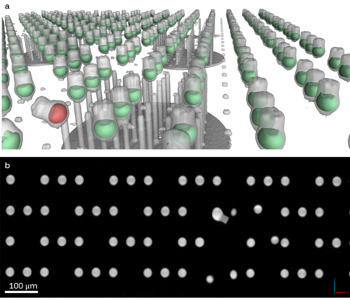
Figure 1. Example of solder ball misalignment in HBM: (a) 3D volume rendering, with the misaligned solder ball highlighted in red; (b) XZ orthogonal slice showing the defective solder ball. Image Credit: Tescan Group
This technique can be used to accurately quantify displacement under thermal stress, a challenge for traditional optical or surface-based measurement techniques.
There is increasing demand for methods able to capture internal geometric changes in three dimensions and under operational conditions as a function of temperature or time.
In this light, a custom setup was designed to enable heating inside the Tescan UniTOM® HR. This approach enabled the acquisition of high-resolution scans, allowing real-time structural evolution to be resolved and facilitating quantitative warpage assessment via a comparative analysis of the resulting datasets at room and elevated temperatures.

This information has been sourced, reviewed and adapted from materials provided by TESCAN.
For more information on this source, please visit TESCAN.