Introduction
Zinc oxide (ZnO) is a wide-gap semiconductor, which is transparent from the visible to infrared regions and is resistant to reductive ambient. Because of these properties, it is expected to be applicable as a material for transparent electrode [1, 2] and window layers of solar cells [3]. Many techniques for the deposition of ZnO, such as sputtering [4-8], spray pyrolysis [9-11] and metal-organic chemical vapor deposition [12-14] have been developed. Among these growth methods of ZnO films, magnetron sputtering is an appropriate method for the growth of uniform and transparent ZnO films at low temperatures [8, 15]. The physical damage due to the impingement of charged particles in this method, however, results in the formation of various defects and gives rise to residual stress in the films. By suppressing the physical damage, high-quality crystalline films with a small residual stress can be obtained. By inserting a mesh grid, which can apply a negative dc bias, between the anode and cathode, glow discharge can be confined to the region between the cathode and the grid. The electron temperature can be lowered in the afterglow region between the cathode and the anode [16] and the impingement of high-energy ions on the substrate surface can be suppressed due to the low space potential in the afterglow region. For the application of the ZnO films to the transparent conductive films, transparent films with low resistivity on the order of 10-4 Ω cm are required. The aluminum(Al) doped ZnO films are usually investigated. The electrical resistivity, however, has not become a low enough value for the transparent conducting electrodes.
In this study, in order to further decrease the film resistivity, co-doping of fluorine (F) to ZnO:Al film was attempted using rf magnetron sputtering apparatus with the mesh grid electrode. The Al doped ZnO (ZnO:Al) target with ZnF2 tablets was sputtered in Ar gas. The contamination of heavy metal atoms from the mesh grid was also investigated.
Experimental Procedure
Figure 1 shows a schematic diagram of the magnetron sputtering apparatus with the mesh grid. The stainless steel grid mesh was coated with zinc plating about 6 μm thickness in order to prevent the contamination of the films by the positive ion bombardment, and was connected to a DC power source. A substrate heater, ceramic heater, was mounted on a heater holder isolated from the chamber. A sintered ceramic target with a mixture of ZnO and Al2O3 (2 wt%) was used. Silicon and glass substrates were mounted on the ceramic heater. The substrates were ultrasonically cleaned in acetone, methyl alcohol and deionized pure water before setting in the chamber. For co-doping of fluorine to ZnO:Al, ZnF2 tablets which were prepared by pressing ZnF2 powder were arranged on erosion area of the target. The dimension of the tablets was 7mm in diameter and 6.5 mm in height. The diameter of the target was approximately 65 mm.
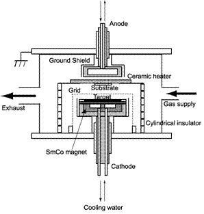
Figure 1. Schematic diagram of rf magnetron sputtering apparatus with a mesh grid.
The experimental conditions are as follows. The distance between the cathode and the grid electrode was 20 mm. The distance between the anode and the mesh grid electrode was also 20 mm. Sputtering was carried out in pure argon with an rf power of 20 W for 90 min. The total gas pressure during deposition was 6mTorr. The substrate temperature during the sputtering was set at room temperature and 60oC. The optimal nagative bias (-40 V) for suppressing the impingement of the charged particles on the substrate was applied to the grid [17].
The film thicknesses of all films were 100-150 nm. The optical transmittance spectra of the films deposited on the glass substrates were measured in the range from 300 to 800 nm using a double-beam visible-ultraviolet spectrophotometer (Simadzu UV365) with a blank substrate (in the reference). Electrical resistivity and carrier concentration were measured at room temperature by the van der Pauw method. The contamination in the films was analyzed using electron probe microanalyser (Shimadzu EPMA-1500). Crystallinity of the film was measured using an X-ray diffractometer (Rigaku, RAD IIIA Cu Kα line) with a thin-film attachment.
Results and Discussion
Table 1 shows the concentration of iron contents in the ZnO films deposited using the mesh grid electrodes with and without zinc plating. As shown in the table, iron wasn't detected in the film deposited using the zinc plated mesh. Plating the Zn film on the mesh grid, contamination of heavy metal atoms from the mesh could be avoided even when the negative grid bias was applied. Such a contamination disturbs the crystallinity. Figure 2 shows the lattice constants along c-axis of the films deposited using the mesh with and without zinc plating as a function of the fraction of oxygen pressure. The lattice constant value of films deposited using the zinc plated mesh grid was approximately the same as that of the bulk ZnO (0.5207 nm) and was smaller than those deposited by the grid without the zinc plating. From this result, it became clear that the suppression of the heavy metal atoms contamination from the mesh by the zinc plating avoided the deterioration of the crystallinity of the ZnO films.
Table 1. Iron contents in the ZnO:Al films deposited using stainless steel meshes with and without zinc plating.
|
|
|
No plating
Zn[at.%]
Fe[at.%]
|
0.400
Zn (Mol %)
Fe (Mol %)
|
|
Zinc plating
|
0
|
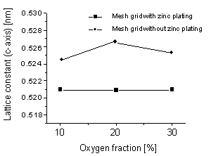
Figure 2. Variation in the lattice constant as a function of oxygen fraction.
Figure 3 shows the optical transmission spectra for F, Al-codoped and ZnO:Al films deposited on glass substrates without heating. As shown in this figure, F, Al-codoped ZnO film was transparent in the visible region (300-800 nm) similarly to the ZnO:Al film. The electrical properties of F, Al-codoped ZnO films were measured using the van der Pauw method. Figure 4 shows the variation in the resistivity and the carrier concentration as a function of the F content. As can be seen in Figure 4, the resistivity decreased from 3 x 10⁻² to 1.4 x 10⁻³ Ωcm as the F content increased. With F contents above approximately 0.6 at.%, however, the resistivity saturated. On the other hand, the carrier concentration of films monotonically increased with F contents. Figure 5 shows the variation in the absorption coefficients as a function of the photon energy (α2 - hν plot). From these data, it is apparent that the optical band gap of the F, Al-codoped ZnO films obtained by α2-hν plots shifted to a larger value of about 0.1 eV compared with that of ZnO:Al. This shift is assumed to be due to the Burstein-Moss effect [18].
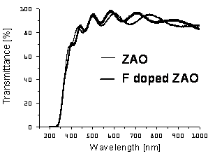
Figure 3. Optical transmission spectra of ZnO:Al and F codoped ZnO:Al films.
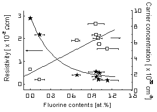
Figure 4. Dependence of the carrier concentration and the resistivity of ZnO:Al and F-codoped ZnO:Al films on the fluorine content.
Figure 5 shows the variation in the optical gap as a function of the F content in the films. As the F content increased, the optical band gap also increased monotonically as in the case of carrier concentration. These results substantiate the occurrence of the Burstein-Moss effect.
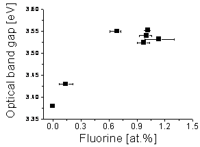
Figure 5. The variation in the optical gap as a function of the F content in the films
Conclusions
F codoping to the ZnO:Al was investigated using a magnetron sputtering apparatus with a grid electrode. The F, Al-codoped ZnO films were transparent in the visible region (380-800 nm) similarly to the ZnO:Al films. The resistivity decreased to 1.4 x 10⁻³ Ωcm as the F content increased. The carrier concentration of the films increased with increasing F content. From the variation in the carrier concentration and the optical gap, occurrence of the Burstein-Moss effect was presumed. Using the magnetron sputtering with a mesh grid plated with zinc, codoping effect in ZnO film with F and Al was confirmed.
Acknowledgements
We would like to thank Prof. K. Kobayashi of Shizuoka University for his beneficial advices on fluorine co-doping.
References
1. R. E. I. Schrop and A. Madan, “Properties of conductive zinc oxide films for transparent electrode applications prepared by rf magnetron sputtering”, J. Appl. Phys., 66 (1989) 2027-2031.
2. M. A. Martinez, J. Herrero and M. T. Gutierrez, “Deposition of transparent and conductive Al-doped ZnO thin films for photovoltaic solar cells”, Sol. Energy Mater. Sol. Cells, 45 (1997) 75-86.
3. J. C. Lee, K. H. Kang, S. K. Kim, K. H. Yoon, I. J. Park and J. Song, “RF sputter deposition of the high-quality intrinsic and n-type ZnO window layers for Cu(In,Ga)Se2-based solar cell applications”, Sol. Energy Mater. Sol. Cells, 64 (2000) 185-195.
4. S. Maniv and A. Zangvil, “Controlled texture of reactively rf-sputtered ZnO thin films”, J. Appl. Phys., 49 (1978) 2787-2792.
5. N. Croitoru, A. Seidman and K. Yassin, “Some physical properties of ZnO sputtered films”, Thin Solid Films, 150 (1987) 291-301.
6. Y. Igasaki and H. Saito, “The effects of deposition rate on the structural and electrical properties of ZnO:Al films deposited on (110) oriented sapphire substrates”, J. Appl. Phys., 70 (1991) 3613-3619.
7. J. H. Jou and M. Y. Han, “Substrate dependent internal stress in sputtered zinc oxide thin films”, J. Appl. Phys., 71 (1992) 4333-4336.
8. K. B. Sundaram and A. Khan, “Characterization and optimization of zinc oxide films by r.f. magnetron sputtering”, Thin Solid Films, 295 (1997) 87-91.
9. P. S. Reddy, G. R. Chetty, S. Uthanna, B. S. Naidu and P. J. Reddy, “Optical properties of spray deposited ZnO films, Solid State Commun. 77 (1991) 899-901.
10. F. D. Paraguay, W. L. Estrada, D. R. N. Acosta, E. Andrade and M. Yoshida, “Growth, structure and optical characterization of high quality ZnO thin films obtained by spray pyrolysis”, Thin Solid Films, 350 (1999) 192-202.
11. M. Purica, E. Budianu, E. Rusu, M. Danila and R. Gavrila, “Optical and structural investigation of ZnO thin films prepared by chemical vapor deposition (CVD)”, Thin Solid Films 403–404 (2002) 485-488.
12. J. S. Kim, H. A. Marzouk, P. J. Reucroft and C. E. Hamrin, “Characterization of high quality c axis oriented ZnO thin films grown by metal organic chemical vapor deposition using zinc acetate as source material”, Thin Solid Films, 217 (1992) 133-137.
13. C. R. Gorla, N. M. Emanetoglu, S. Liang, W. E. Mayo, Y. Lu, M. Wraback and H. Shen, “Structural, optical, and surface acoustic wave properties of epitaxial ZnO films grown on (012) sapphire by metalorganic chemical vapor deposition”, J. Appl. Phys., 85 (1999) 2595-2602.
14. Y. Kashiwaba, F. Katahira, K. Haga, T. Sekiguchi and H. Watanabe, “Hetero-epitaxial growth of ZnO thin films by atmospheric pressure CVD method”,J. Cryst. Growth, 221 (2000) 431-434.
15. R. Ondo-Ndong, F. Pascal-Delannoy, A. Boyer, A. Giani and A. Foucaran, “Structural properties of zinc oxide thin films prepared by r.f. magnetron sputtering”, Mater. Sci. & Eng. B, 97 (2003) 68-73.
16. K. Yasui, N. Ninagawa and T. Akahane, “Improvement of the Crystallinity of 3C-SiC Films by Lowering the Electron Temperatures in Afterglow Plasma Region Using Triode Plasma CVD”, J. Electron. Mater., 26 (1997) 178-182.
17. K. Yasui, N. V. Phuong, Y. Kuroki, M. Takata and T. Akahane, “Improvement in Crystallinity of ZnO Films Prepared by rf Magnetron Sputtering with Grid Electrode”, Jpn. J. Appl. Phys., 40 (2005) 684-687.
18. E. Burstein, “Anomalous Optical Absorption Limit in InSb”, Phys. Rev., 93 (1986) 632-633.
Contact Details
|