A new embodied AI experimentalist named Qumus moves beyond digital reasoning, using robotics, computer vision, and multi-agent planning to create graphene, recover from lab errors, and assemble atomically thin devices in the physical world.
A new embodied AI experimentalist named Qumus moves beyond digital reasoning, using robotics, computer vision, and multi-agent planning to create graphene, recover from lab errors, and assemble atomically thin devices in the physical world.
Researchers have introduced Qumus, an autonomous, physically embodied artificial intelligence (AI) experimentalist in quantum materials. Their study, posted on the arXiv preprint server, combines generative AI with robotics to independently perform hypothesis generation, experiment execution, error correction, and data analysis.
The novel AI system is reported to have achieved the first AI-driven fabrication of complex atomically thin nanodevices, including a graphene field-effect transistor produced through vdW stacking without human intervention. Using a multi-agent AI architecture, Qumus autonomously produced graphene flakes, fabricated nanodevices, and performed experimentation, demonstrating a self-improving framework for accelerated quantum materials discovery.
Challenges in Quantum Material Development
The field of two-dimensional (2D) quantum materials began with the mechanical exfoliation of graphene in 2004, introducing a range of atomically thin materials with unique electronic and optical properties. Many-layered crystals can be separated into single-atomic sheets and assembled into custom heterostructures that exhibit new quantum behavior. These structures are useful for advanced semiconductor and optoelectronic technologies.
However, practical development has been limited by complex laboratory workflows. Conventional processing relies on manual synthesis, visual flake identification, and precise manipulation of microscopic structures. These procedures are time-consuming, dependent on humans, and often suffer from poor reproducibility. Additionally, many advanced quantum materials are sensitive to air exposure, making repeated manual handling impractical.
Multi-Agent Framework
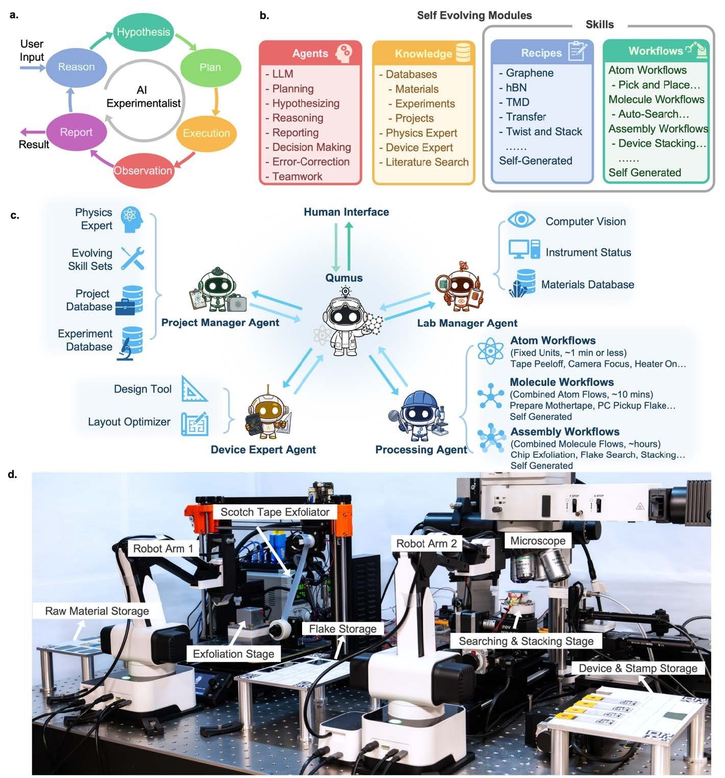
To mimic the collaborative structure of a human research team, Qumus employs a hierarchical multi-agent large language model (LLM) network controlled by a central coordinator. The main agent interprets user instructions, assigns tasks, and manages goals.
Specialized sub-agents support distinct functions. The Project Manager Agent analyzes previous experiments and literature to suggest fabrication methods. The Lab Manager Agent monitors laboratory inventory using computer vision. Similarly, the Device Expert Agent designs device layouts, while the Processing Agent executes laboratory operations.
The Processing Agent operates through three levels. Atom Workflows execute actions such as stage movement, camera focusing, and temperature adjustment. Molecule Workflows combine these actions into larger tasks, such as chip exfoliation. At the same time, Assembly Workflows integrate multiple procedures into complete fabrication processes.
The robotic platform includes a tape exfoliation system that transfers crystal layers onto silicon chips using automated Scotch tape processing. Two robotic arms move materials between storage areas and temperature-controlled vacuum stages.
The workstation contains an optical microscope with automated magnification and motorized focusing for submicron alignment during layer transfer. Computer vision systems support laboratory monitoring and microscopic analysis. Overhead cameras using YOLOv8 (You Only Look Once version 8) instance segmentation to track tools and QR-coded material carriers. A rule-based vision system analyzes RGB microscope images, applies edge detection, and estimates flake thickness using color distance measurements.
Experimental Capabilities
To evaluate its ability to function as an independent experimental system, Qumus was tasked with isolating a graphene flake larger than 200 μm2. Starting with an empty experimental database, the AI explored a four-dimensional (4D) parameter space that included stage temperature, contact time, massage cycles, and tape peeling speed.
During a continuous experiment lasting over 4 hours, the robotics system analyzed previous outcomes and iteratively adjusted parameters. After five optimization cycles, it successfully isolated a graphene flake measuring 245 μm2.
The platform demonstrated resilience during unexpected disruptions. In one experiment involving hexagonal boron nitride (hBN), a researcher removed a silicon chip during processing without notifying the system. The platform detected the missing substrate, generated a recovery strategy, and initiated re-exfoliation on a replacement chip. When the language model incorrectly labeled an hBN flake as graphene, Qumus recognized that no hBN flake had been recorded and adjusted its plan to isolate the correct material.
Additionally, the system fabricated a complete graphene field-effect transistor. The Device Expert Agent selected suitable graphene and hBN flakes for a substrate containing pre-patterned metal contacts. The Processing Agent then performed a 90-minute dry transfer procedure involving 30 physical operations and 18 decision-making stages. Using real-time image analysis and Newton’s rings detection, the robot successfully identified the contact point and assembled an aligned hBN-graphene heterostructure over the electrodes.
Implications for Advanced Device Manufacturing
The automation of 2D material processing opens new potential for efficient manufacturing of advanced electronic devices. By reducing manual handling, the system can accelerate the screening and optimization of vdW heterostructures. Integrating these robotic platforms into inert gas environments could support the processing of highly air-sensitive materials.
The platform also provides a foundation for digital material databases. Each experiment records metadata linking optical measurements, exfoliation parameters, alignment conditions, device records, and fabrication outcomes. This data collection can support machine learning (ML) models that automatically refine fabrication procedures, thereby improving reproducibility and reducing reliance on manual trial-and-error.
Conclusion: Autonomous Scientific Research
In summary, Qumus addresses key challenges in nanomanufacturing and quantum materials science. By transforming 2D material fabrication from a manual process into an automated workflow, this approach could significantly shorten the time required to move from theoretical concepts to functional quantum devices. The system can coordinate multiple agents, optimize fabrication procedures, and construct a graphene field-effect transistor within about 90 minutes.
Although current performance is limited by hardware factors such as mechanical movement speed, optical focusing, and thermal equilibration, researchers noted that the underlying multi-agent framework is highly scalable. Future work should focus on faster robotic systems and improved thermal control. Linking multiple robotic laboratories via shared digital networks could enable global collaboration and accelerate the development of quantum electronics and materials. However, the authors present these results as initial demonstrations, with broader validation across additional materials and devices still needed.
Download your PDF copy by clicking here.
Disclaimer: The views expressed here are those of the author expressed in their private capacity and do not necessarily represent the views of AZoM.com Limited T/A AZoNetwork the owner and operator of this website. This disclaimer forms part of the Terms and conditions of use of this website.
Source:
- Shi, L., et al. (2026). Qumus: Realization of an Embodied AI Quantum Material Experimentalist. arXiv, 2605.18407. DOI: 10.48550/arXiv.2605.18407, https://arxiv.org/abs/2605.18407