Jun 23 2009
To address the challenges of wafer polishing at future technology nodes, Peter Wolters GmbH, a wholly-owned subsidiary of Novellus Systems (NASDAQ:NVLS), has recently developed advanced polishing technology for its MicroLine AC 1500-P3 and AC 2000-P3 double-sided silicon wafer polishing (DSP) systems that will meet the lithography requirements for semiconductor device manufacturing at 22nm and beyond.
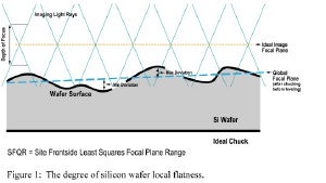
With current state-of-the-art semiconductor manufacturers beginning to enter 32nm high-volume manufacturing, leading manufacturers of wafer polishing equipment are already considering the planarity requirements for silicon wafers at the 22nm technology node. At these next generation nodes, extremely tight requirements are being placed on both the shape of the prime wafer and the flatness of its surface. Since semiconductor device structures are patterned using optical lithography, the achievable process window or depth of focus becomes governed by the flatness of the area being exposed by the optical beam. The "degree of silicon wafer local flatness" as measured by the Site Frontside Least Squares Focal Plane Range metric defines the acceptable level of silicon wafer surface planarity for use in advanced IC manufacturing. Lithography processes require the SFQR value to be much smaller than the depth of focus. To meet the current needs of 32nm lithography, the SFQR-max value is typically less than 30nm for a site size of 26 mm x 8 mm with an edge exclusion of 2 mm. A double-sided silicon wafer polish is required to achieve low SFQR values at these advanced nodes. Another significant challenge during the polishing step is to control wafer planarity (parallel front and back wafer surfaces) while preventing the pad from rounding the edge of the wafer.
Peter Wolters has engineered advanced, patent-pending sensor and process control capabilities into its latest polishing systems, allowing the AC-1500 P3 and the AC-2000 P3 to achieve SFQR-max values of less than 20nm -a requirement for 22nm lithography. Excellent front to backside parallelism is achieved using stress-free guidance of the wafer throughout the polish step. The process control enabled by this new technology delivers a more homogeneous polishing process with no edge rounding out to 1 mm of edge exclusion. When used for today's 4Xnm and 3Xnm production, the MicroLine's flatter wafers widen the depth of focus process window, resulting in improved critical dimension control. This larger process window increases patterning yield and lithography productivity through better scanner-to-scanner matching and reduced qualification and set-up time.
"The in-situ data obtained by the MicroLine's temperature and eddy current sensors allow us to adjust the process parameters to match the polishing consumables with the incoming wafer geometry," said Kay Petersen, executive vice president of Novellus' Industrial Applications group. "Our silicon wafer polish systems are ready today to enable 22nm lithography development."