Sep 22 2009
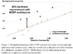
Novellus Systems (NASDAQ: NVLS) announced today that it has developed a multiple wavelength UV Thermal Processing (UVTP) treatment on the company's SOLA platform that results in a 25 percent improvement in film hardness compared to a single wavelength treatment of the same k-value dielectric.
At 32nm and beyond, ultra-low dielectric constant (ULK) materials must be introduced into the semiconductor manufacturing process flow in order to improve device performance. ULK materials, however, present challenges associated with adhesion and the mechanical properties of the film. Adhesion issues are typically addressed through interface engineering, while mechanical properties are improved using a UVTP treatment. UVTP processing results in a lower bulk dielectric constant (k), cross-links the chemical "backbone" (which increases mechanical strength), and removes porogen (pore generation material) from non-dense ULK films. Increasing the mechanical strength of the film ensures that it will withstand downstream manufacturing processes such as chemical-mechanical planarization (CMP) and final packaging.
It is well known that porous ULK materials require different process steps for porogen removal and cross-linking. The unique SOLA UV treatment utilizes Novellus' multi-station sequential processing (MSSP) architecture to independently optimize the porogen removal and cross-linking steps, while maintaining high system throughput. Wavelength, temperature, treatment time, and UV intensity can be independently controlled at each of the four processing stations.
Cohesive and adhesive failures during CMP and final packaging steps can be exacerbated by increasing the number of ULK layers in the interconnect stack. A margin of safety in the packaging process can be ensured by tailoring the assembly process and design rules; however, optimizing the bulk film properties (i.e. hardness, modulus and residual stress) is also required. Figure 2 shows the difference between soft and hard ULK films used in a simulated interconnect stack. Eight layers of an IMD/barrier stack were deposited on a bare wafer to simulate a ULK interconnect structure. For a given post-treatment film stress, the softer film shows peeling and delamination at the wafer edge, while the harder film shows none.
"Controlling the UV exposure parameters is critical to obtaining the maximum mechanical performance of a given dielectric constant film," said Boaz Kenane, director of technology for UVTP at Novellus. "SOLA UVTP with MSSP enables the independent optimization of key UV treatment steps to enhance film performance while maintaining a high level of manufacturability."