Researchers at the Max Planck Institute and the Fraunhofer Institute demonstrate how atomic layer processing can enhance the optical performance of photonic devices made of SiC.
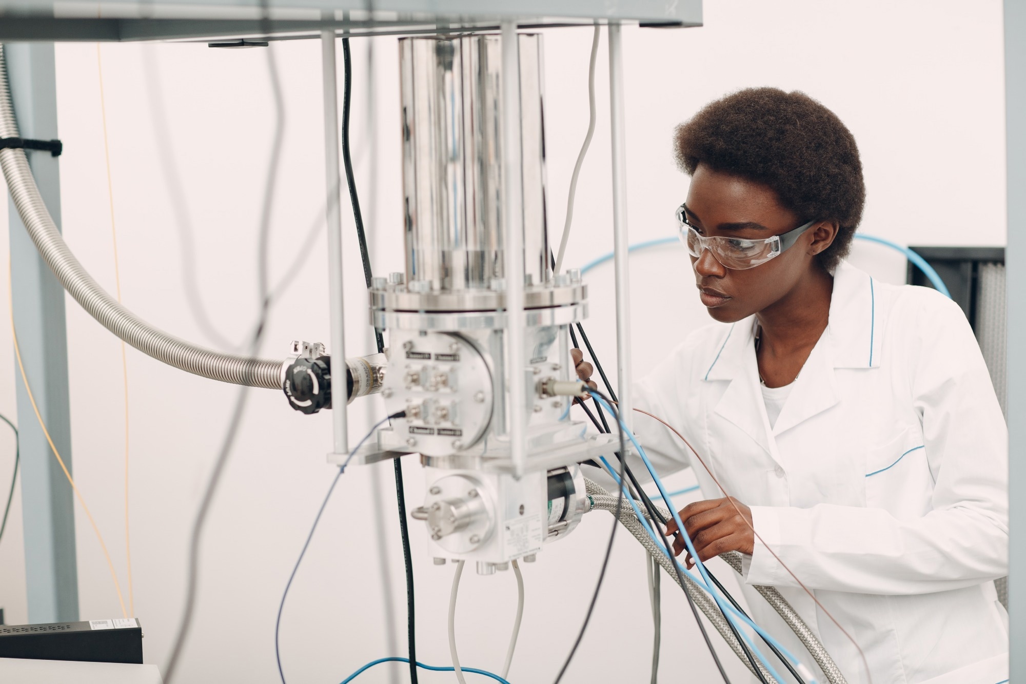 Image Credit:Max4e Photo /Shutterstock.com
The teams from both institutes (Max Planck Institute for the Science of Light (MPL) and the Fraunhofer Institute for Integrated Systems and Device Technology IISB) are collaborating on the design of highly efficient photonic circuits.
Silicon carbide (SiC) is a promising material platform for photonic integrated circuits (PICs) and compact solid-state quantum systems.
Quantum systems are likely to be a prominent feature in future technologies. Major high-tech corporations, particularly institutional investors, are participating in a worldwide competition to translate the principles of quantum mechanics from research labs into broader practical applications. Evolutions in tech have already begun in information processing, sensors, and communication technology.
From a technological standpoint, quantum systems can be best characterized as an integration of quantum physics, photonics, and electronics. The quantum computer is certainly the most well-known illustration of this concept. Presently, quantum systems still largely resemble intricate optoelectronic laboratory configurations, necessitating significant technical effort to generate, manipulate, and process quantum states.
The complexity and substantial size present limiting factors, and the cooling requirements pose a challenge, as many existing solutions operate effectively only at temperatures near absolute zero.
The incorporation of quantum technologies into commercially viable products and services requires substantial research and development to establish foundational technologies. Likewise, the economic realization of functional quantum systems is hindered by the lack of a consistent, future-proof material platform that would enable significant progress in miniaturization, improved performance, and cost reduction.
Connectable and Quantum-Compatible: Silicon Carbide as a Quantum Material
Owing to its distinctive physical properties, silicon carbide (SiC) is a promising technological foundation for solid-state quantum systems. SiC is classified as a wide bandgap (WBG) semiconductor and has gained recognition in recent years, especially within the domain of power electronics.
Additionally, it is highly appealing for the development of photonic microsystems and photonic integrated circuits (PICs) due to its capability to produce optical devices, light sources, and sensors. Moreover, SiC attracts attention for its nonlinear optical effects, which can be used to alter the color of laser light.
For example, it can efficiently convert infrared light into visible light. The potential for integrating point defects in the form of color centers that operate at room temperature suggests that SiC may even facilitate the direct incorporation of quantum functionality in the future.
This makes silicon carbide an ideal platform for photonics, electronics, and quantum applications.
Dr. Pascal Del'Haye, Project Head, Max Planck Institute for the Science of Light
Silicon carbide (SiC) can thus be used to create all the necessary components for the development of robust, compact quantum systems. It is compatible with both microelectronics and microphotonics, providing novel quantum electronic capabilities. Given its compatibility with CMOS processes in traditional silicon technology, SiC is well-suited for large-scale industrial production of quantum photonic integrated circuits (PICs).
Optimization of the First Microphotonic Devices Leads to SiC Quantum Chips
There remains a considerable distance to traverse before optoelectronic quantum chips are realized, and the research in this domain is still largely in its early stages. To construct Photonic Integrated Circuits (PICs), standardized microphotonics devices that exhibit minimal optical losses are required. Essential to this are optical waveguides and ring resonators that efficiently guide or store light within diminutive structures.
While waveguides serve as loss-free optical conduits, resonators are composed of small rings where the input light can complete up to a million cycles. The photon storage durations achieved through this method permit these devices to be charged with substantial circulating optical power, facilitating a range of nonlinear optical phenomena.
For instance, micro-resonators can transform laser light at a specific wavelength into an optical frequency comb, a light source composed of several discrete frequencies, applicable for extremely rapid parallel data transmission in telecommunications networks.
Another beneficial effect is the interaction of counter-propagating light. The nonlinear optical coupling of counter-propagating light within ring resonators results in spontaneous symmetry breaking, allowing light to circulate in a singular direction, either clockwise or counterclockwise. This phenomenon can be used, for example, to create chip-integrated optical diodes, photonic switches, or optical sensors, which facilitate the development of more intricate photonic systems.
The quality of photonic devices produced on Silicon Carbide (SiC) substrates is not yet optimal, and the relatively high surface roughness leads to optical losses in waveguides and resonators. Perfect surfaces are crucial to ensure that photons can travel swiftly and do not escape outward. A promising approach is to refine the component surfaces through atomic layer etching (ALE) to establish well-defined interfaces and reduce loss and scattering centers.
Bridging the Gap Between Basic Research and Process Development in the ALP-4-Sic Project
To establish a new manufacturing process for intricate photonic devices using silicon carbide, it is essential that fundamental and application-focused research collaborate closely. Within the ALP-4-SiC initiative – which focuses on atomic layer processing for SiC in the realms of photonics and quantum communication – the MPL in Erlangen and the Fraunhofer IISB, along with its Fraunhofer Technology Center for High-Performance Materials THM in Freiberg, are combining their specialized knowledge.
The MPL possesses significant expertise in the design and evaluation of photonic components, whereas the IISB offers proficiency in SiC semiconductor technology and atomic-layer processing.
The innovative strategy of merging atom-layer-based techniques for photonic devices, which exhibit markedly enhanced optical characteristics, holds substantial promise for the future commercialization of integrated photonic devices.