A research team comprising Jeong Yong Lee and Jong Min Yuk from the Korea Advanced Institute of Science and Technology (KAIST) together with research groups of Paul Alivisatos and Alex Zettl from the University of California, Berkeley (UC Berkeley) has devised a technique to study processes taking place in liquid media on a scale below 1 nm.
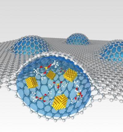 Two sheets of graphene encapsulate a platinum growth solution. (Credit: KAIST)
The researchers have developed a graphene liquid capsule or cell (GLC) for a transmission electron microscope (TEM) to perform in-situ and real-time imaging of nanoscale processes occurring in fluids at an atomic-scale resolution.
The graphene liquid cell (GLC) consists of an ultra-thin liquid film of a platinum growth solution sandwiched by two graphene sheets. The thickness of each graphene layer was one atom, which is the thinnest ever been used of liquid cell fabrication. The researchers closely looked into the GLC to monitor the dynamics and growth of platinum nanocrystals in the solution as they grew in size through coalescence without affecting the graphene chamber containing the ultra-thin liquid film.
By imaging the details at atomic-scale resolution, the research team was able to determine significant features during the coalescence process of the nanocrystals that made them to grow into specific shapes.
Yuk explained that this research will help study other phenomena of materials in a fluid state such as biological, chemical and physical phenomena at the atomic-scale resolution, thus showing promise to several future applications. However, a GLC TEM’s full application to biological samples is not yet verified as more investigations on liquid microscopy are yet to come. Nevertheless, the GLC is the highly efficient technology available today to maintain the natural stage of fluid species in the liquid to help perform a TEM imaging.
Researchers tried electron-transparent membranes of silicon oxide or silicon nitride to make liquid capsules. The comparatively higher thickness of these liquid capsules results in inferior electron transmittance and resolution. The thickness of silicon nitride is 25 nm, while that of graphene is merely 0.34 nm.
The study results have been reported in the journal, Science.