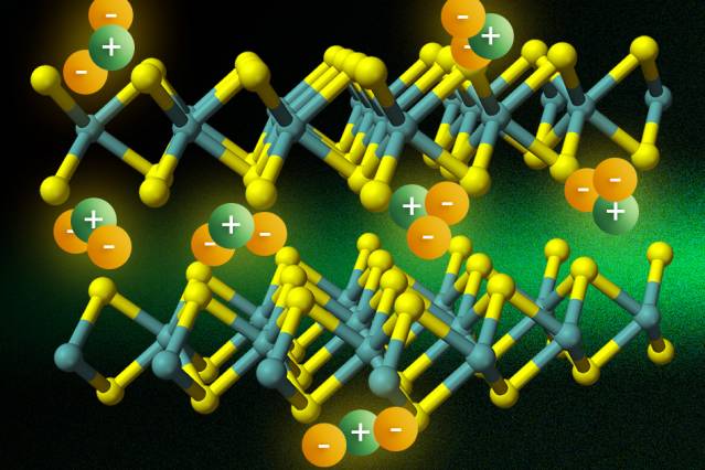
 Shown here is the crystal structure of molybdenite, MoS2. When hit with a burst of laser light, freed electrons and holes combine to form combinations called trions, consisting of two electrons and one hole (represented here by orange and green balls). Illustration: Jose-Luis Olivares/MIT
Its common knowledge in electronics that shining a light on semiconductor materials like silicon used in computer chips or solar cells, will result in higher conductivity. MIT researchers have now discovered a distinct two-dimensional semiconductor which has the opposite effect.
The researchers created time-delayed terahertz pulses to investigate the material’s conductive response, with the help of intense laser pulses illuminated on the MoS2 layer. It was found that the original conductivity of the semiconductor layer was reduced by one third.
By measuring the transmission of the terahertz radiation through the material, we can extract its electrical conductivity. This approach is more convenient than conventional methods that attach electrical contacts to the samples and measure the current.
Nuh Gedik, MIT postdoc
When a semiconductor is illuminated by light, pairs of loose holes and electrons are generated because of light absorption, facilitating electric current flow via the material. As a result, the conductivity of the material increases. Several optoelectronic devices such as light detectors, digital cameras, and solar cells are optimized and designed based on this principle. However, the researchers realized the opposite effect in a two-dimensional semiconductor.
The team members said that atomically thin layered crystal is the material of interest for various applications in recent times due to their strong charge carriers confinement in a two-dimensional plane. This remarkable property enhances the electrostatic interactions within the carriers, resulting in the formation of an exciton. In reality, excitons formed in the MoS2 layer trap extra free electrons and generate bound state called trions, using one hole and two electrons.
The illumination of light on MoS2 layer, therefore, transforms free electrons into trions with heavier mass and same net charge as that of an electron. Trions, reported as an intrinsic crystal property, are generally unstable and formed at low temperatures, lasting for a short time period. However, in the MoS2 layer, strong trionic effect is produced at room temperature, that can be detected through the team’s ultrafast terahertz technique.
The team said that this approach facilitates the introduction of next-generation wireless excitonic devices at room temperature. Further research involves the investigation of other two-dimensional materials, which exhibit the same photoconduction and trionic effects.
The research work published in Physical Review Letters was supported by the National Science Foundation and the U.S. Department of Energy.
References