Samsung Electronics Co., Ltd., the world’s leading producer of semiconductor and display solutions, formally opened the doors to its new Device Solutions America headquarters here today, setting the stage for a new wave of innovation across the digital landscape.
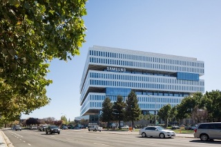 Samsung Electronics Device Solutions America HQ campus occupies 9.4 acres featuring a 10-story office/labs facility. (Photo: Business Wire)
Located on the same corner in San Jose’s tech corridor where Samsung’s original campus was first built more than 30 years ago, the new headquarters symbolizes both Samsung’s long heritage in Silicon Valley and the company’s focus on innovation and growth.
Samsung Electronics’ semiconductor operations have long been at the forefront of innovation and with the new America headquarters, Samsung’s R&D efforts will be bolstered substantially. Innovation and advanced technologies for next-generation devices generated at the new facility will help make an even greater contribution to providing the critical competitive advantages that the company’s U.S. and global customers seek.
Speaking before an audience of more than 800 at the site’s Grand Opening ceremony, Oh-Hyun Kwon, Vice Chairman and CEO of Samsung Electronics, said, “We are transforming Samsung into a world-class example of a truly market-focused technology company.” He further said that the company is “laying the groundwork for a more aggressive pace of growth over the next several decades.”
While Samsung Electronics’ Device Solutions Division has experienced explosive growth since its arrival in Silicon Valley in 1983, it has created multiple organizations dispersed throughout the region. The move brings more than 700 employees together on a 1.1-million-square-foot campus, enhancing efficiency that is crucial in creating products and solutions at the cutting edge of technology. The main facility will house various research labs dedicated to semiconductors, LEDs and displays, as well as staff in sales, marketing and other support areas.
Complete with gardens and open air space within the building, its new design increases collaboration by encouraging more spontaneous encounters between staff, while also bringing nature closer to the workplace to increase employees’ contentment and creativity.
Samsung’s President of its Device Solutions America operations, Jaesoo Han, said, “Today represents a major milestone as we open our most strategically important Samsung facility in the U.S. and also our biggest investment in Silicon Valley.” He went on to say that “Samsung’s goal is nothing less than to develop the best next-generation technologies for device solutions.”
Dignitaries in attendance at the grand opening for Samsung’s new headquarters included the current mayor of San Jose—the Honorable Sam Liccardo, former San Jose mayor—the Honorable Chuck Reed, State Senator Bob Wieckowski, San Jose State University President Susan Martin, and San Francisco Korean Consul General Dongman Han.
In keeping with the company’s corporate social responsibility (CSR) initiatives, Samsung announced a number of contributions at the event that will further support the Silicon Valley community. The company donated $100,000 to the Family Giving Tree and another $100,000 to the Second Harvest Food Bank.
Samsung Electronics has also established a $1 million STEM College Education Scholarship Fund to celebrate its latest expansion. Deserving university students who are currently enrolled in STEM-focused programs at a California State or University of California school will benefit from this program, beginning with a $50,000 gift to San Jose State University this year. Each scholarship will cover tuition and living expenses for one year.
Samsung Electronics’ Device Solutions CSR programs are focused on enhancing health, education and sustainability opportunities for children. In addition to opening its new state-of-the-art facility in San Jose, Samsung is dedicated to supporting the local community and helping to inspire the next generation of innovators with volunteer staff support and corporate donations.
For more information, visit www.samsung.com/us/samsungGOC15