Mar 21 2016
The Department of Energy’s (DOE) Oak Ridge National Laboratory (ORNL) has developed a new processing technique for two-dimensional (2D) electronic devices. This new technique has the potential to reduce the power consumption of the devices, and to increase their efficiency and mechanical flexibility.
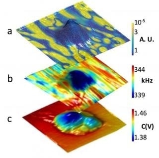 This diagram illustrates the effect of helium ions on the mechanical and electrical properties of the layered ferroelectric: a.) Disappearance domains in the exposed area; as the mound forms yellow regions (ferroelectricity) gradually disappear; b.) Mechanical properties of the material; warmer colors indicate hard areas, cool colors indicate soft areas; c.) Conductivity enhancement; warmer colors show insulating areas, cooler colors show more conductive areas. (Credit: ORNL)
A research team under the leadership of Olga Ovchinnikova of ORNL's Center for Nanophase Materials Sciences Division employed a helium ion microscope, which is an atomic-scale "sandblaster," on a layered ferroelectric surface of bulk copper indium thiophosphate. The result, to their surprise, was the discovery of a material with attributes that could be useful for photvoltaics, phones, screens, and flexible electronics.
Our method opens pathways to direct-write and edit circuitry on 2D material without the complicated current state-of-the-art multi-step lithographic processes.
Olga Ovchinnikova, Center for Nanophase Materials Sciences Division, ORNL
She and her colleague Alex Belianinov demonstrated that the helium ion microscope could be used to manage ferroelectric domain distribution, improve conductivity, and grow nanostructures, although the microscope’s typical use is to cut and shape matter. Their work could establish a path to replace silicon as the choice for semiconductors in some applications.
Everyone is looking for the next material - the thing that will replace silicon for transistors. 2-D devices stand out as having low power consumption and being easier and less expensive to fabricate without requiring harsh chemicals that are potentially harmful to the environment.
Alex Belianinov, ORNL
Reducing power consumption by using 2-D-based devices could be as significant as improving battery performance.
Imagine having a phone that you don't have to recharge but once a month.
Olga Ovchinnikova, Center for Nanophase Materials Sciences Division, ORNL
This research was funded through the Laboratory Directed Research and Development program. Some of the work was performed at the Center for Nanophase Materials Sciences, a DOE Office of Science User Facility.